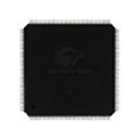
CY7C09579V-83AXC Cypress Semiconductor Corp, CY7C09579V-83AXC Datasheet - Page 7

CY7C09579V-83AXC
Manufacturer Part Number
CY7C09579V-83AXC
Description
IC,SYNC SRAM,32KX36,CMOS,QFP,144PIN,PLASTIC
Manufacturer
Cypress Semiconductor Corp
Specifications of CY7C09579V-83AXC
Format - Memory
RAM
Memory Type
SRAM - Dual Port, Synchronous
Memory Size
1.152M (32K x 36)
Speed
83MHz
Interface
Parallel
Voltage - Supply
3 V ~ 3.6 V
Operating Temperature
0°C ~ 70°C
Package / Case
144-LQFP
Density
1.125Mb
Access Time (max)
18ns
Sync/async
Synchronous
Architecture
SDR
Clock Freq (max)
45MHz
Operating Supply Voltage (typ)
3.3V
Address Bus
15b
Package Type
TQFP
Operating Temp Range
0C to 70C
Number Of Ports
2
Supply Current
360mA
Operating Supply Voltage (min)
3.135V
Operating Supply Voltage (max)
3.465V
Operating Temperature Classification
Commercial
Mounting
Surface Mount
Pin Count
144
Word Size
36b
Number Of Words
32K
Lead Free Status / RoHS Status
Lead free / RoHS compliant by exemption
Lead Free Status / RoHS Status
Lead free / RoHS compliant by exemption
Available stocks
Company
Part Number
Manufacturer
Quantity
Price
Company:
Part Number:
CY7C09579V-83AXC
Manufacturer:
Cypress Semiconductor Corp
Quantity:
10 000
Maximum Ratings
Exceeding maximum ratings may shorten the useful life of the
device. User guidelines are not tested.
Storage temperature.................................... –65
Ambient temperature with
power applied ................................................–55
Supply voltage to ground potential ................... –0.5 V to +4.6 V
DC voltage applied to
outputs in High Z state..............................–0.5 V to V
DC input voltage ....................................–0.5 V to V
Output current into outputs (LOW) .................................. 20 mA
Electrical Characteristics
Over the Operating Range
Capacitance
Document Number: 38-06054 Rev. *E
V
V
V
V
I
I
I
I
I
I
Parameter
C
C
Notes
OZ
CC
SB1
SB2
SB3
SB4
6. The voltage on any input or I/O pin can not exceed the power pin during power-up.
7. Pulse width < 20 ns.
OH
OL
IH
IL
IN
OUT
Parameter
Output HIGH Voltage (V
Output LOW Voltage (V
Input HIGH Voltage
Input LOW Voltage
Output Leakage Current
Operating Current (V
Standby Current (Both Ports TTL Level) CE
Standby Current (One Port TTL Level) CE
Standby Current (Both Ports CMOS Level)
CE
Standby Current (One Port CMOS Level)
CE
L
L
& CE
| CE
R
R
V
[6]
V
IH
DD
Input capacitance
Output capacitance
, f = f
– 0.2V, f = 0
DD
MAX
DD
DD
= Max., I
Description
Description
= Min., I
= Min., I
OUT
OL
OH
C to +150
C to +125
DD
= +4.0 mA)
= 0 mA) Outputs Disabled
= –4.0 mA)
DD
+ 0.5 V
L
+ 0.5 V
L
| CE
& CE
T
C
[7]
R
C
A
R
V
= 25
V
IH
IH
Static discharge voltage............................................... > 2001 V
Latch-up current ..........................................................> 200 mA
Operating Range
Test Conditions
, f = f
Commercial
, f = f
C, f = 1 MHz, V
Range
MAX
MAX
Min
–10
2.4
2.0
–
–
–
–
–
–
–
DD
= 3.3 V
0.01
-100
Typ
250
170
150
30
–
–
–
–
–
0
Temperature
Ambient
C to +70
CY7C09569V
CY7C09579V
Max
385
220
200
0.4
0.8
10
75
–
–
1
Max
10
10
Min
–10
2.4
2.0
C
–
–
–
–
–
–
–
CY7C09569V
CY7C09579V
0.01
Typ
240
160
140
-83
25
–
–
–
–
–
3.3 V 165 mV
V
Max
360
210
190
Page 7 of 32
0.4
0.8
10
70
DD
Unit
–
–
1
pF
pF
Unit
mA
mA
mA
mA
mA
A
V
V
V
V
[+] Feedback


