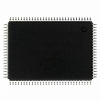
CY7C1463AV33-133AXC Cypress Semiconductor Corp, CY7C1463AV33-133AXC Datasheet - Page 12

CY7C1463AV33-133AXC
Manufacturer Part Number
CY7C1463AV33-133AXC
Description
CY7C1463AV33-133AXC
Manufacturer
Cypress Semiconductor Corp
Datasheet
1.CY7C1463AV33-133AXI.pdf
(34 pages)
Specifications of CY7C1463AV33-133AXC
Format - Memory
RAM
Memory Type
SRAM - Synchronous
Memory Size
36M (2M x 18)
Speed
133MHz
Interface
Parallel
Voltage - Supply
2.375 V ~ 2.625 V
Operating Temperature
0°C ~ 70°C
Package / Case
100-LQFP
Lead Free Status / RoHS Status
Lead free / RoHS Compliant
Other names
428-2026
Available stocks
Company
Part Number
Manufacturer
Quantity
Price
Company:
Part Number:
CY7C1463AV33-133AXC
Manufacturer:
CYPRESSSE
Quantity:
3 287
Company:
Part Number:
CY7C1463AV33-133AXC
Manufacturer:
Cypress Semiconductor Corp
Quantity:
10 000
Truth Table
The truth table for CY7C1461AV33/CY7C1463AV33/CY7C1465AV33 follows.
Notes
Document #: 38-05356 Rev. *I
Deselect Cycle
Deselect Cycle
Deselect Cycle
Continue Deselect Cycle
Read Cycle (Begin Burst)
Read Cycle (Continue Burst)
NOP/Dummy Read
(Begin Burst)
Dummy Read (Continue Burst)
Write Cycle (Begin Burst)
Write Cycle (Continue Burst)
NOP/Write Abort (Begin Burst)
Write Abort (Continue Burst)
Ignore Clock Edge (Stall)
Sleep Mode
2. X = “Don't Care.” H = logic HIGH, L = logic LOW. BWx = L signifies at least one byte write select is active, BWx = Valid signifies that the desired byte write selects
3. Write is defined by BW
4. When a write cycle is detected, all IOs are tri-stated, even during byte writes.
5. The DQs and DQP
6. CEN = H, inserts wait states.
7. Device powers up deselected and the IOs in a tri-state condition, regardless of OE.
8. OE is asynchronous and is not sampled with the clock rise. It is masked internally during write cycles. During a read cycle DQs and DQP
are asserted, see truth table for details.
is inactive or when the device is deselected, and DQs and DQP
Operation
X
pins are controlled by the current cycle and the OE signal. OE is asynchronous and is not sampled with the clock.
X
, and WE. See truth table for read or write.
Address
External
External
External
Current
Used
None
None
None
None
None
None
Next
Next
Next
Next
CE
H
X
X
X
X
L
L
X
L
X
X
X
X
L
1
X
CE
= data when OE is active.
H
X
H
H
H
X
X
L
X
X
X
X
X
X
2
CE
H
X
X
X
X
X
X
L
L
X
L
L
X
X
3
ZZ ADV/LD WE
H
L
L
L
L
L
L
L
L
L
L
L
L
L
H
H
H
H
H
X
X
L
L
L
L
L
L
L
CY7C1463AV33, CY7C1465AV33
[2, 3, 4, 5, 6, 7, 8]
X
X
X
X
H
X
H
X
X
X
X
X
L
L
BW
X
X
X
X
X
X
X
X
H
H
X
X
L
L
X
OE
X
X
X
X
H
H
X
X
X
X
X
X
L
L
CEN CLK
H
X
L
L
L
L
L
L
L
L
L
L
L
L
CY7C1461AV33
X
L->H Tri-State
L->H Tri-State
L->H Tri-State
L->H Tri-State
L->H Data Out
L->H Data Out
L->H Tri-State
L->H Tri-State
L->H Data In (D)
L->H Data In (D)
L->H Tri-State
L->H Tri-State
L->H
= Tri-state when OE
X
Tri-State
Page 12 of 34
DQ
(Q)
(Q)
–
[+] Feedback


