CY7C1463AV33-133AXC Cypress Semiconductor Corp, CY7C1463AV33-133AXC Datasheet - Page 4
CY7C1463AV33-133AXC
Manufacturer Part Number
CY7C1463AV33-133AXC
Description
CY7C1463AV33-133AXC
Manufacturer
Cypress Semiconductor Corp
Datasheet
1.CY7C1463AV33-133AXI.pdf
(34 pages)
Specifications of CY7C1463AV33-133AXC
Format - Memory
RAM
Memory Type
SRAM - Synchronous
Memory Size
36M (2M x 18)
Speed
133MHz
Interface
Parallel
Voltage - Supply
2.375 V ~ 2.625 V
Operating Temperature
0°C ~ 70°C
Package / Case
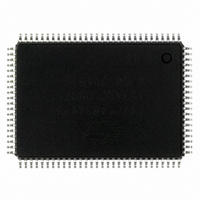
100-LQFP
Lead Free Status / RoHS Status
Lead free / RoHS Compliant
Other names
428-2026
Available stocks
Company
Part Number
Manufacturer
Quantity
Price
Company:

Part Number:
CY7C1463AV33-133AXC
Manufacturer:
CYPRESSSE
Quantity:
3 287
Company:
Part Number:
CY7C1463AV33-133AXC
Manufacturer:
Cypress Semiconductor Corp
Quantity:
10 000


Contents
Pin Configurations ........................................................... 5
Pin Definitions .................................................................. 9
Functional Overview ...................................................... 10
Interleaved Burst Address Table
(MODE = Floating or VDD) ............................................. 11
Linear Burst Address Table (MODE = GND) ................ 11
ZZ Mode Electrical Characteristics ............................... 11
Truth Table ...................................................................... 12
Truth Table for Read/Write ............................................ 13
Truth Table for Read/Write ............................................ 13
Truth Table for Read/Write ............................................ 13
IEEE 1149.1 Serial Boundary Scan (JTAG) .................. 14
TAP Controller State Diagram ....................................... 14
TAP Controller Block Diagram ...................................... 14
TAP Timing ...................................................................... 16
TAP AC Switching Characteristics ............................... 17
Document #: 38-05356 Rev. *I
Single Read Accesses .............................................. 10
Burst Read Accesses ................................................ 10
Single Write Accesses ............................................... 11
Burst Write Accesses ................................................ 11
Sleep Mode ............................................................... 11
Disabling the JTAG Feature ...................................... 14
Test Access Port (TAP) ............................................. 14
PERFORMING A TAP RESET .................................. 14
TAP REGISTERS ...................................................... 14
TAP Instruction Set ................................................... 15
3.3 V TAP AC Test Conditions ....................................... 18
3.3 V TAP AC Output Load Equivalent ......................... 18
2.5 V TAP AC Test Conditions ....................................... 18
2.5 V TAP AC Output Load Equivalent ......................... 18
TAP DC Electrical Characteristics and
Operating Conditions ..................................................... 18
Identification Register Definitions ................................ 19
Scan Register Sizes ....................................................... 19
Identification Codes ....................................................... 19
165-ball FBGA Boundary Scan Order .......................... 20
209-ball FBGA Boundary Scan Order .......................... 21
Maximum Ratings ........................................................... 22
Operating Range ............................................................. 22
Electrical Characteristics ............................................... 22
Capacitance .................................................................... 23
Thermal Resistance ........................................................ 23
Switching Characteristics .............................................. 24
Switching Waveforms .................................................... 25
Ordering Information ...................................................... 28
Package Diagrams .......................................................... 29
Document History Page ................................................. 32
Sales, Solutions, and Legal Information ...................... 34
Ordering Code Definitions ......................................... 28
Worldwide Sales and Design Support ....................... 34
Products .................................................................... 34
PSoC Solutions ......................................................... 34
CY7C1463AV33, CY7C1465AV33
CY7C1461AV33
Page 4 of 34
[+] Feedback
Related parts for CY7C1463AV33-133AXC
Image
Part Number
Description
Manufacturer
Datasheet
Request
R

Part Number:
Description:
Manufacturer:
Cypress Semiconductor Corp
Datasheet:
Part Number:
Description:
Manufacturer:
Cypress Semiconductor Corp
Datasheet:
Part Number:
Description:
Manufacturer:
Cypress Semiconductor Corp
Datasheet:
Part Number:
Description:
Manufacturer:
Cypress Semiconductor Corp
Datasheet:
Part Number:
Description:
Manufacturer:
Cypress Semiconductor Corp
Datasheet: