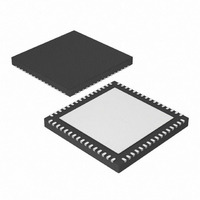
DSPIC33FJ64GP706AT-I/MR Microchip Technology, DSPIC33FJ64GP706AT-I/MR Datasheet - Page 178

DSPIC33FJ64GP706AT-I/MR
Manufacturer Part Number
DSPIC33FJ64GP706AT-I/MR
Description
16 Bit MCU/DSP 40MIPS 64KB FLASH 64 QFN 9x9x0.9mm T/R
Manufacturer
Microchip Technology
Series
dsPIC™ 33Fr
Datasheet
1.DSPIC33FJ64GP206A-IMR.pdf
(338 pages)
Specifications of DSPIC33FJ64GP706AT-I/MR
Core Processor
dsPIC
Core Size
16-Bit
Speed
40 MIPs
Connectivity
CAN, I²C, IrDA, LIN, SPI, UART/USART
Peripherals
AC'97, Brown-out Detect/Reset, DMA, I²S, POR, PWM, WDT
Number Of I /o
53
Program Memory Size
64KB (64K x 8)
Program Memory Type
FLASH
Ram Size
16K x 8
Voltage - Supply (vcc/vdd)
3 V ~ 3.6 V
Data Converters
A/D 18x10b/12b
Oscillator Type
Internal
Operating Temperature
-40°C ~ 85°C
Package / Case
64-VFQFN, Exposed Pad
Lead Free Status / RoHS Status
Lead free / RoHS Compliant
Eeprom Size
-
Lead Free Status / RoHS Status
Lead free / RoHS Compliant
- Current page: 178 of 338
- Download datasheet (3Mb)
dsPIC33FJXXXGPX06A/X08A/X10A
15.1
Configure the Output Compare modes by setting the
appropriate Output Compare Mode (OCM<2:0>) bits in
the Output Compare Control (OCxCON<2:0>) register.
Table 15-1 lists the different bit settings for the Output
Compare modes. Figure 15-2 illustrates the output
compare operation for various modes. The user
TABLE 15-1:
FIGURE 15-2:
DS70593B-page 178
OCM<2:0>
000
001
010
011
100
101
110
111
Active-High One-Shot
Active-Low One-Shot
(OCM = 110 or 111)
Delayed One-Shot
Continuous Pulse
Output Compare Modes
(OCM = 001)
(OCM = 010)
(OCM = 011)
(OCM = 100)
(OCM = 101)
Module Disabled
Active-Low One-Shot
Active-High One-Shot
Toggle
Delayed One-Shot
Continuous Pulse
PWM without Fault Protection
PWM with Fault Protection
OUTPUT COMPARE MODES
Toggle
TMRy
PWM
OUTPUT COMPARE OPERATION
OCxRS
OCxR
Mode
Output Compare
Mode Enabled
Current output is maintained
Controlled by GPIO register
Preliminary
‘1’, if OCxR is non-zero
‘1’, if OCxR is non-zero
OCx Pin Initial State
‘0’, if OCxR is zero
‘0’, if OCxR is zero
Timer is Reset on
Period Match
0
1
0
0
application must disable the associated timer when
writing to the Output Compare Control registers to
avoid malfunctions.
Note:
See Section 13. “Output Compare”
(DS70209) in the “dsPIC33F/PIC24H
Family Reference Manual” for OCxR and
OCxRS register restrictions.
OCx rising edge
OCx falling edge
OCx rising and falling edge
OCx falling edge
OCx falling edge
No interrupt
OCFA falling edge for OC1 to OC4
OCx Interrupt Generation
2009 Microchip Technology Inc.
—
Related parts for DSPIC33FJ64GP706AT-I/MR
Image
Part Number
Description
Manufacturer
Datasheet
Request
R

Part Number:
Description:
Manufacturer:
Microchip Technology Inc.
Datasheet:

Part Number:
Description:
Manufacturer:
Microchip Technology Inc.
Datasheet:

Part Number:
Description:
Manufacturer:
Microchip Technology Inc.
Datasheet:

Part Number:
Description:
Manufacturer:
Microchip Technology Inc.
Datasheet:

Part Number:
Description:
Manufacturer:
Microchip Technology Inc.
Datasheet:

Part Number:
Description:
Manufacturer:
Microchip Technology Inc.
Datasheet:

Part Number:
Description:
Manufacturer:
Microchip Technology Inc.
Datasheet:

Part Number:
Description:
Manufacturer:
Microchip Technology Inc.
Datasheet:


