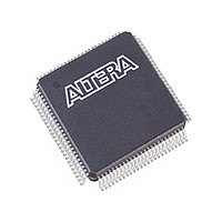
EPM570GT100I5N Altera, EPM570GT100I5N Datasheet - Page 20

EPM570GT100I5N
Manufacturer Part Number
EPM570GT100I5N
Description
MAX II
Manufacturer
Altera
Datasheet
1.EPM570GT100I5N.pdf
(88 pages)
Specifications of EPM570GT100I5N
Family Name
MAX II
Memory Type
Flash
# Macrocells
440
Frequency (max)
1.8797GHz
Propagation Delay Time
8.7ns
Number Of Logic Blocks/elements
57
# I/os (max)
76
Operating Supply Voltage (typ)
1.8V
In System Programmable
Yes
Operating Supply Voltage (min)
1.71V
Operating Supply Voltage (max)
1.89V
Operating Temp Range
-40C to 100C
Operating Temperature Classification
Industrial
Mounting
Surface Mount
Pin Count
100
Package Type
TQFP
Lead Free Status / Rohs Status
Compliant
Available stocks
Company
Part Number
Manufacturer
Quantity
Price
Company:
Part Number:
EPM570GT100I5N
Manufacturer:
ALTERA
Quantity:
52
Company:
Part Number:
EPM570GT100I5N
Manufacturer:
ALTERA
Quantity:
170
2–12
MultiTrack Interconnect
MAX II Device Handbook
The Quartus II software automatically creates carry chain logic during design
processing, or you can create it manually during design entry. Parameterized
functions such as LPM functions automatically take advantage of carry chains for the
appropriate functions. The Quartus II software creates carry chains longer than 10 LEs
by linking adjacent LABs within the same row together automatically. A carry chain
can extend horizontally up to one full LAB row, but does not extend between LAB
rows.
Clear and Preset Logic Control
LAB-wide signals control the logic for the register ’s clear and preset signals. The LE
directly supports an asynchronous clear and preset function. The register preset is
achieved through the asynchronous load of a logic high. MAX II devices support
simultaneous preset/asynchronous load and clear signals. An asynchronous clear
signal takes precedence if both signals are asserted simultaneously. Each LAB
supports up to two clears and one preset signal.
In addition to the clear and preset ports, MAX II devices provide a chip-wide reset pin
(DEV_CLRn) that resets all registers in the device. An option set before compilation in
the Quartus II software controls this pin. This chip-wide reset overrides all other
control signals and uses its own dedicated routing resources (that is, it does not use
any of the four global resources). Driving this signal low before or during power-up
prevents user mode from releasing clears within the design. This allows you to control
when clear is released on a device that has just been powered-up. If not set for its chip-
wide reset function, the DEV_CLRn pin is a regular I/O pin.
By default, all registers in MAX II devices are set to power-up low. However, this
power-up state can be set to high on individual registers during design entry using
the Quartus II software.
In the MAX II architecture, connections between LEs, the UFM, and device I/O pins
are provided by the MultiTrack interconnect structure. The MultiTrack interconnect
consists of continuous, performance-optimized routing lines used for inter- and intra-
design block connectivity. The Quartus II Compiler automatically places critical
design paths on faster interconnects to improve design performance.
The MultiTrack interconnect consists of row and column interconnects that span fixed
distances. A routing structure with fixed length resources for all devices allows
predictable and short delays between logic levels instead of large delays associated
with global or long routing lines. Dedicated row interconnects route signals to and
from LABs within the same row. These row resources include:
■
■
The DirectLink interconnect allows an LAB to drive into the local interconnect of its
left and right neighbors. The DirectLink interconnect provides fast communication
between adjacent LABs and/or blocks without using row interconnect resources.
DirectLink interconnects between LABs
R4 interconnects traversing four LABs to the right or left
© October 2008 Altera Corporation
Chapter 2: MAX II Architecture
MultiTrack Interconnect


