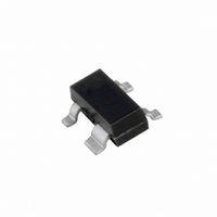
BAT74,215 NXP Semiconductors, BAT74,215 Datasheet

BAT74,215
Specifications of BAT74,215
933742290215
BAT74 T/R
Related parts for BAT74,215
BAT74,215 Summary of contents
Page 1
BAT74 Schottky barrier double diode Rev. 03 — 19 April 2010 1. Product profile 1.1 General description Planar Schottky barrier double diode with an integrated guard ring for stress protection. Two electrically isolated Schottky barrier diodes, encapsulated in a small ...
Page 2
... NXP Semiconductors 3. Ordering information Table 3. Type number Package BAT74 4. Marking Table 4. Type number BAT74 [ made in Hong Kong * = p: made in Hong Kong * = t: made in Malaysia * = W: made in China 5. Limiting values Table 5. In accordance with the Absolute Maximum Rating System (IEC 60134). Symbol Per diode FRM ...
Page 3
... NXP Semiconductors 6. Thermal characteristics Table 6. Symbol R th(j-a) [1] Refer to SOT143B standard mounting conditions. 7. Characteristics Table amb Symbol Per diode Temperature coefficient of forward voltage −0.6 %/K. [1] [2] Pulse test: t [3] When switched from I BAT74_3 Product data sheet Thermal characteristics Parameter thermal resistance from junction to ambient Characteristics ° ...
Page 4
... NXP Semiconductors (mA (1) (2) (3) 1 − 0.4 = 125 °C (1) T amb = 85 °C (2) T amb = 25 °C (3) T amb Fig 1. Forward current as a function of forward voltage; typical values (pF ° MHz; T amb Fig 3. Diode capacitance as a function of reverse voltage; typical values BAT74_3 Product data sheet ...
Page 5
... NXP Semiconductors 8. Test information D.U. Ω × ( Fig 5. Reverse recovery time test circuit and waveforms 9. Package outline Fig 6. 10. Packing information Table 8. The indicated -xxx are the last three digits of the 12NC ordering code. Type number BAT74 [1] For further information and the availability of packing methods, see ...
Page 6
... NXP Semiconductors 11. Soldering 0.7 (3×) 0.7 Fig 7. 4.6 Fig 8. BAT74_3 Product data sheet 3.25 0.6 (3×) 0.5 (3×) 1.9 0.6 (3×) 0.6 0.75 0.95 0.9 1 Reflow soldering footprint BAT74 (SOT143B) 4.45 2.2 2.575 1.2 Wave soldering footprint BAT74 (SOT143B) All information provided in this document is subject to legal disclaimers. ...
Page 7
... Release date BAT74_3 20100419 • Modifications: The format of this data sheet has been redesigned to comply with the new identity guidelines of NXP Semiconductors. • Legal texts have been adapted to the new company name where appropriate. • Section 1.1 “General • Table 1 “Quick reference • ...
Page 8
... In no event shall NXP Semiconductors be liable for any indirect, incidental, punitive, special or consequential damages (including - without limitation - lost profits, lost savings, business interruption, costs related to the removal or ...
Page 9
... NXP Semiconductors Quick reference data — The Quick reference data is an extract of the product data given in the Limiting values and Characteristics sections of this document, and as such is not complete, exhaustive or legally binding. 14. Contact information For more information, please visit: For sales office addresses, please send an email to: ...
Page 10
... NXP Semiconductors 15. Contents 1 Product profile . . . . . . . . . . . . . . . . . . . . . . . . . . 1 1.1 General description . . . . . . . . . . . . . . . . . . . . . 1 1.2 Features and benefits . . . . . . . . . . . . . . . . . . . . 1 1.3 Applications . . . . . . . . . . . . . . . . . . . . . . . . . . . 1 1.4 Quick reference data . . . . . . . . . . . . . . . . . . . . 1 2 Pinning information . . . . . . . . . . . . . . . . . . . . . . 1 3 Ordering information . . . . . . . . . . . . . . . . . . . . . 2 4 Marking . . . . . . . . . . . . . . . . . . . . . . . . . . . . . . . . 2 5 Limiting values Thermal characteristics . . . . . . . . . . . . . . . . . . 3 7 Characteristics . . . . . . . . . . . . . . . . . . . . . . . . . . 3 8 Test information . . . . . . . . . . . . . . . . . . . . . . . . . 5 9 Package outline . . . . . . . . . . . . . . . . . . . . . . . . . 5 10 Packing information . . . . . . . . . . . . . . . . . . . . . 5 11 Soldering ...


