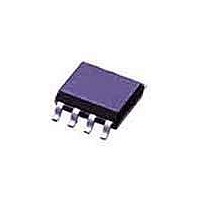
TISP61089AD Bourns Inc., TISP61089AD Datasheet - Page 2

TISP61089AD
Manufacturer Part Number
TISP61089AD
Description
SCRs Dual P Gate Forward Conducting
Manufacturer
Bourns Inc.
Datasheet
1.TISP61089ADR-S.pdf
(8 pages)
Specifications of TISP61089AD
Breakover Current Ibo Max
11 A
Rated Repetitive Off-state Voltage Vdrm
120 V
Off-state Leakage Current @ Vdrm Idrm
0.005 mA
Holding Current (ih Max)
150 mA
Mounting Style
SMD/SMT
Package / Case
SOIC-8
Lead Free Status / RoHS Status
Lead free / RoHS Compliant
Available stocks
Company
Part Number
Manufacturer
Quantity
Price
Part Number:
TISP61089AD
Manufacturer:
BOURNS/伯恩斯
Quantity:
20 000
Company:
Part Number:
TISP61089ADR
Manufacturer:
BOURNS
Quantity:
3 085
Part Number:
TISP61089ADR
Manufacturer:
BOURNS/伯恩斯
Quantity:
20 000
Part Number:
TISP61089ADR-S
Manufacturer:
BOURNS/伯恩斯
Quantity:
20 000
These ‘61089 parts are all dual forward-conducting buffered p-gate thyristor (SCR) overvoltage protectors. They are designed to protect
monolithic SLICs (Subscriber Line Interface Circuits) against overvoltages on the telephone line caused by lightning, a.c. power contact and
induction. The ‘61089 limits voltages that exceed the SLIC supply rail voltage. The ‘61089 parameters are specified to allow equipment
compliance with Telcordia (formally Bellcore) GR-1089-CORE and ITU-T recommendations K.20, K.21 and K.45.
The SLIC line driver section is typically powered from 0 V (ground) and a negative (battery) voltage. The protector gate is connected to this
negative supply. This references the protection (clipping) voltage to the negative supply voltage. The protection voltage will then track the
negative supply voltage and the overvoltage stress on the SLIC is minimized.
Positive overvoltages are clipped to ground by diode forward conduction. Negative overvoltages are initially clipped close to the SLIC
negative supply rail value. If sufficient current is available from the overvoltage, then the protector SCR will switch into a low voltage on-state
condition. As the overvoltage subsides the high holding current of ‘61089 SCR avoids d.c. latchup.
The ‘61089 is intended to be used with a series resistance of at least 25 Ω and a suitable overcurrent function for Telcordia compliance. Power
fault conditions require a series overcurrent element which either interrupts or reduces the circuit current before the ‘61089 current rating is
exceeded. For equipment compliant to ITU-T recommendations K.20 or K.21 or K.45 only, the series resistor value is set by the coordination
requirements. For coordination with a 400 V limit GDT, a minimum series resistor value of 10 Ω is recommended.
The ‘61089 buffered gate design reduces the loading on the SLIC supply during overvoltages caused by power cross and induction. The
regular pin-out for surface mount and through-hole packages is a feed through configuration. Connection to the SLIC is made via the ‘61089,
Ring through pins 4 - 5 and Tip through pins 1 - 8. A non-feed-through surface mount (D) package is available. This shunt (SD) version pin-out
does not make duplicate connections to pin 5 and pin 8 which increases package creepage distance from ground of the other connections
from about 0.7 mm to over 3 mm. High voltage ringing SLICs, with battery voltages below -100 V and down to -155 V, can be protected by the
TISP61089B device. Details of this device are in the TISP61089B data sheet.
Absolute Maximum Ratings, -40
Repetitive peak off-state voltage, V
Repetitive peak gate-cathode voltage, V
Non-repetitive peak on-state pulse current (see Notes 1 and 2)
Non-repetitive peak on-state current, V
Non-repetitive peak gate current, 1/2 µs pulse, cathodes commoned (see Notes 1 and 2)
Operating free-air temperature range
Junction temperature
Storage temperature range
NOTES: 1. Initially the protector must be in thermal equilibrium with -40 °C ≤ T
Description
TISP61089 Gated Protector Series
10/1000 µs (Telcordia (Bellcore) GR-1089-CORE, Issue 2, February 1999, Section 4)
5/320 µs (ITU-T K.20, K.21& K.45, K.44 open-circuit voltage wave shape 10/700 µs)
1.2/50 µs (Telcordia (Bellcore) GR-1089-CORE, Issue 2, February 1999, Section 4)
2/10 µs (Telcordia (Bellcore) GR-1089-CORE, Issue 2, February 1999, Section 4)
0.1 s
1 s
5 s
300 s
900 s
2. The rated current values may be applied either to the Ring to Ground or to the Tip to Ground terminal pairs. Additionally, both
to its initial conditions. Gate voltage ranges are -20 V to -75 V for the ‘61089 and -20 V to -100 V for the ‘61089A.
terminal pairs may have their rated current values applied simultaneously (in this case the Ground terminal current will be twice
the rated current value of an individual terminal pair). Above 85 °C, derate linearly to zero at 150 °C lead temperature.
GK
= 0
°
GG
C
KA
= -75 V, 50 Hz to 60 Hz (see Notes 1 and 2)
≤
= 0
T J
Rating
≤
85
°
C (Unless Otherwise Noted)
J
≤ 85 °C. The surge may be repeated after the device returns
Customers should verify actual device performance in their specific applications.
‘61089A
‘61089A
61089
61089
Symbol
V
V
I
I
PPSM
I
GKRM
GSM
T
TSM
DRM
T
T
stg
A
J
Specifications are subject to change without notice.
-40 to +150
-40 to +150
-40 to +85
NOVEMBER 1995 - REVISED JULY 2008
Value
-100
-120
-120
0.95
0.93
+40
-85
100
120
4.8
2.7
30
40
11
Unit
°C
°C
°C
V
V
A
A
A


