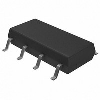
S-35399A03-J8T2G Seiko Instruments, S-35399A03-J8T2G Datasheet - Page 33

S-35399A03-J8T2G
Manufacturer Part Number
S-35399A03-J8T2G
Description
Real Time Clock 2-wire Real Time Clock
Manufacturer
Seiko Instruments
Datasheet
1.S-35399A03-J8T2G.pdf
(53 pages)
Specifications of S-35399A03-J8T2G
Supply Voltage (max)
3 V
Supply Voltage (min)
1.3 V
Maximum Operating Temperature
+ 85 C
Minimum Operating Temperature
- 40 C
Mounting Style
SMD/SMT
Rtc Bus Interface
Serial
Supply Current
0.34 uA
Package / Case
SOP-8
Lead Free Status / RoHS Status
Lead free / RoHS Compliant
Rev.2.0
The followings are Read/Write in the S-35399A03.
(1) Data Read in S-35399A03
After detecting a start condition, the S-35399A03 receives device code and command. The S-35399A03 enters the
Read-data mode by the Read/Write bit “1”. The data is output from B7 in 1-byte. Input an acknowledgment signal
from the master device every moment that the S-35399A03 outputs 1-byte data. However, do not input an
acknowledgment signal (input NO_ACK) for the last data-byte output from the master device. This procedure
notifies the completion of Read. Next, input a stop condition to the S-35399A03 to finish access.
_00
SDA
SCL
3-byte data
Code + command
0
1
1
SDA
SCL
1
1-byte data
0
: Input from master device
: Output from S-35399A03
0
Figure 35 Example of Data Read 1 (1-Byte Data Register)
Figure 36 Example of Data Read 2 (3-Byte Data Register)
1
: Input from master device
: Output from S-35399A03
1
1
Code + command
0
R/W
1
9
1
B7
1
0
0
Seiko Instruments Inc.
0
0 1
B0
R/W
B7
9
B7
18
Input NO_ACK after the 1st byte
of data has been output.
B0
B0
Input NO_ACK after the 3rd byte of data
has been output.
18
B7
27
2-WIRE REAL-TIME CLOCK
B0
36
S-35399A03
33


