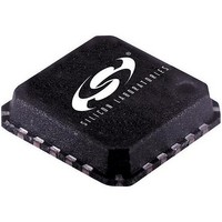
SI5310-BMR Silicon Laboratories Inc, SI5310-BMR Datasheet - Page 14

SI5310-BMR
Manufacturer Part Number
SI5310-BMR
Description
Clock Generators & Support Products Multiplier/Regenratr 155MHz 622MHz
Manufacturer
Silicon Laboratories Inc
Type
Precision Clock Multiplier/ Regenerator ICr
Datasheet
1.SI5310-C-GM.pdf
(26 pages)
Specifications of SI5310-BMR
Mounting Style
SMD/SMT
Description/function
Precision Clock Multiplier/ Regenerator IC
Package / Case
MLP-20
Lead Free Status / RoHS Status
Lead free / RoHS Compliant
Si5310
4.1. DSPLL
The PLL structure (shown in Figure 1 on page 5) utilizes
Silicon Laboratories' DSPLL
superior jitter performance while eliminating the need
for external loop filter components found in traditional
PLL implementations. This is achieved by using a digital
signal processing (DSP) algorithm to replace the loop
filter commonly found in analog PLL designs. This
algorithm processes the phase detector error term and
generates a digital control value to adjust the frequency
of
technology produces clocks with less jitter than is
generated using traditional methods. In addition,
because external loop filter components are not
required, sensitive noise entry points are eliminated,
thus making the DSPLL less susceptible to board-level
noise sources.
4.2. Clock Multiplier
The DSPLL phase locks to the clock input signal
(CLKIN) and generates an output clock (MULTOUT) at
a multiple of the input clock frequency. The MULTOUT
output is configured to operate in either the 150–
167 MHz frequency range or in the 600–668 MHz
frequency range using the MULTSEL control input as
indicated in Table 9. Values for typical applications are
given in Table 10.
The amount of jitter present in the MULTOUT output is a
function of the DSPLL jitter transfer function and jitter
generation characteristic. Details are provided in the
PLL Performance section of this document. (See
Figures 4 and 5.) The amount of jitter that the DSPLL
can tolerate on the CLKIN input is specified in Tables 5
and 6.
The DSPLL implementation in the Si5310 is insensitive
to the duty cycle of the CLKIN input. The MULTOUT
output will continue to exhibit a very good duty cycle
characteristic even when the CLKIN input duty cycle is
degraded.
4.3. 1x Multiplication
The Si5310 Clock Multiplier function may also be
utilized as a 1x multiplier in order to provide jitter
attenuation
multiplication of the input clock frequency.
Note: When the Si5310 is configured as a 1:1 multiplier, the
4.4. Clock Regeneration
The DSPLL is used to regenerate a jitter-attenuated
version of the CLKIN input, resulting in a “clean”
CLKOUT output with sharp rising and falling edges. The
14
the
CLKOUT output is not valid.
voltage-controlled
and
®
duty
cycle
®
oscillator
technology to produce
correction
(VCO).
without
The
Rev. 1.3
CLKOUT output is a resampled version of the CLKIN
input
synchronously with the rising edges of the MULTOUT
output. The rising edges of CLKOUT are insensitive to
the location of the falling edges of the CLKIN input.
Thus the period of CLKOUT, measured rising edge to
rising edge, is not affected by the CLKIN duty cycle or
by jitter on the falling edge of CLKIN.
The falling edges of CLKOUT may be affected by the
location of the CLKIN falling edges as follows: If the
duty cycle error of CLKIN is significant relative to the
period of MULTOUT, then
1. The CLKOUT duty cycle may deviate from 50% (the falling
2. Jitter on the falling edges of CLKIN may result in a
Note: When the Si5310 is configured as a 1:1 multiplier, the
4.5. Reference Clock
The Si5310 CMU requires an external reference clock
applied to the REFCLK input for normal device
operation. When REFCLK is absent, the LOL alarm will
always be asserted when it has been determined that
no activity exists on REFCLK, indicating the lock status
of the PLL is unknown. Additionally, the reference clock
input is used to center the DSPLL and also to act as a
reference for determination of the PLL lock status.
REFCLK is a multiple of the CLKIN frequency, and can
be provided in any one of five frequency ranges (9.375–
10.438 MHz, 18.78–20.875 MHz, 37.500–41.750 MHz,
75.00–83.50 MHz, or 150–167.00 MHz). The REFCLK
rate is automatically detected by the Si5310, so no
control inputs are needed for REFCLK frequency
selection. The REFCLK input may be synchronous or
asynchronous with respect to the CLKIN input. The
frequency relationship between REFCLK and CLKIN is
indicated in Table 9. In many applications, it may be
desirable to tie REFCLK and CLKIN together and drive
them from the same clock source. The Si5310 is
insensitive to the phase relationship between CLKIN
and REFCLK, so these differential inputs may be driven
in phase or 180° out of phase if this simplifies board
layout. Values for typical applications are given in
Table 10.
4.6. DSPLL Lock Detection (Loss-of-Lock)
The Si5310 provides lock-detect circuitry that indicates
whether the DSPLL has achieved frequency lock with
the incoming CLKIN signal. The circuit compares the
frequency of a divided down version of the multiplier
edge of CLKOUT will be time quantized to the nearest
rising edge of MULTOUT.)
CLKOUT duty cycle that alternates between two discrete
values.
CLKOUT output is not valid.
with
all
CLKOUT
transitions
occurring


