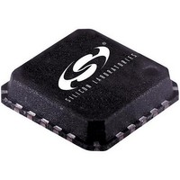
SI5310-BMR Silicon Laboratories Inc, SI5310-BMR Datasheet - Page 15

SI5310-BMR
Manufacturer Part Number
SI5310-BMR
Description
Clock Generators & Support Products Multiplier/Regenratr 155MHz 622MHz
Manufacturer
Silicon Laboratories Inc
Type
Precision Clock Multiplier/ Regenerator ICr
Datasheet
1.SI5310-C-GM.pdf
(26 pages)
Specifications of SI5310-BMR
Mounting Style
SMD/SMT
Description/function
Precision Clock Multiplier/ Regenerator IC
Package / Case
MLP-20
Lead Free Status / RoHS Status
Lead free / RoHS Compliant
output with the frequency of the supplied reference
clock. If the divided multiplier output frequency deviates
from that of the reference clock by the amount specified
in Table 4 on page 8, the PLL is declared out of lock,
and the loss-of-lock (LOL) pin is asserted high. In this
state, the PLL will periodically try to reacquire lock with
the input clock (CLKIN). During reacquisition, the
multiplier output clock (MULTOUT) may drift over a
±600 ppm range relative to the applied reference clock
and the LOL output alarm may toggle until the PLL has
reacquired frequency lock. Due to the low noise and
stability of the DSPLL, under the condition where the
input clock is removed from the inputs, there is the
possibility that the PLL will not drift enough to render an
out-of-lock condition.
If REFCLK is removed, the LOL output alarm will always
be asserted when it has been determined that no
activity exists on REFCLK, indicating the frequency lock
status of the PLL is unknown.
Note: LOL is not asserted during PWRDN/CAL.
4.7. PLL Performance
The Si5310 DSPLL circuitry is designed to provide low
jitter generation, high jitter tolerance, and a well-
controlled jitter transfer function with low peaking. Each
of these key performance parameters is described more
fully in the following sections.
4.7.1. Jitter Tolerance
Jitter tolerance for the Si5310 is defined as the
maximum peak-to-peak sinusoidal jitter that can be
added to the incoming clock before the PLL exceeds its
allowable operating range and loses lock. The tolerance
is a function of the jitter frequency, the incoming clock
rate, and the MULTSEL setting.
The jitter tolerance for specified jitter frequencies and
input clock rates is given in Tables 5 and 6.
4.7.2. Jitter Transfer
Jitter transfer is defined as the ratio of output signal jitter
to input signal jitter for a specified jitter frequency. The
jitter transfer characteristic determines the amount of
input clock jitter that will be passed on to the Si5310
CLKOUT
technology used in the Si5310 provides a tightly
controlled jitter transfer curve because many of the PLL
gain parameters are determined by digital signal
processing algorithms which do not vary over supply
voltage, process, and temperature. In a system
application, a well-controlled transfer curve minimizes
the output clock jitter variation from board to board,
providing
performance.
The jitter transfer characteristic is a function of the
and
more
MULTOUT
consistent
outputs.
system
The
level
DSPLL
jitter
Rev. 1.3
MULTSEL setting and the input clock rate. Higher input
clock rates produce higher bandwidth transfer functions
with lower jitter peaking. Table 4 gives the 3 dB
bandwidth and peaking values for specified input clock
rates and MULTSEL settings. Figures 4 and 5 show a
family of jitter transfer curves for different input clock
rates.
4.7.3. Jitter Generation
Jitter generation is defined as the amount of jitter
produced at the output of the device with a jitter free
input clock. Generated jitter arises from sources within
the VCO and other PLL components. Jitter generation is
a function of MULTSEL setting and input clock
frequency. For clock multiplier applications, the higher
the multiplier ratio desired, the larger the jitter
generation. Table 4 gives the jitter generation values for
specified MULTSEL settings and input clock rates.
4.8. Device Powerdown
The Si5310 PWRDN/CAL input can be used to hold the
device in a power-down state when not in use. When
the PWRDN/CAL input is asserted (set high), the
CLKOUT and MULTOUT output drivers are disabled
and the positive and negative terminals of the CLKOUT
and MULTOUT outputs are each tied to VDD through
100 Ω on-chip resistors. This feature is useful in
reducing power consumption in applications that
employ redundant clock sources. When PWRDN/CAL is
released (set to low) the digital logic is reset to a known
initial condition and the DSPLL circuitry is recalibrated
and will begin to lock to the incoming clock.
4.9. PLL Self-Calibration
Si5310 device provides an internal self-calibration
function that optimizes the loop gain parameters within
the internal DSPLL. Self-calibration is initiated by a
high-to-low transition of the PWRDN/CAL signal while a
valid reference clock is supplied to the REFCLK input.
For optimal jitter performance, the supply voltage
should be stable at 2.5 V ±10% when calibration is
initiated. The PWRDN/CAL signal should be held high
for at least 1 μS after the supply has stabilized before
transitioning low to initiate self-calibration. See Silicon
Laboratories application note AN42 for suggested
methods of generating the PWRDN/CAL signal for
initiation of self-calibration.
4.10. Device Grounding
The Si5310 uses the GND pad on the bottom of the 20-
pin micro leaded package (MLP) for device ground. This
pad should be connected directly to the analog supply
ground. See Figures 11 and 12 for the ground (GND)
pad location.
Si5310
15


