IRFP17N50LPBF Vishay, IRFP17N50LPBF Datasheet - Page 2
IRFP17N50LPBF
Manufacturer Part Number
IRFP17N50LPBF
Description
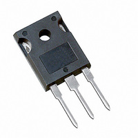
MOSFET N-CH 500V 16A TO-247AC
Manufacturer
Vishay
Specifications of IRFP17N50LPBF
Transistor Polarity
N-Channel
Fet Type
MOSFET N-Channel, Metal Oxide
Fet Feature
Standard
Rds On (max) @ Id, Vgs
320 mOhm @ 9.9A, 10V
Drain To Source Voltage (vdss)
500V
Current - Continuous Drain (id) @ 25° C
16A
Vgs(th) (max) @ Id
5V @ 250µA
Gate Charge (qg) @ Vgs
130nC @ 10V
Input Capacitance (ciss) @ Vds
2760pF @ 25V
Power - Max
220W
Mounting Type
Through Hole
Package / Case
TO-247-3 (Straight Leads), TO-247AC
Minimum Operating Temperature
- 55 C
Configuration
Single
Resistance Drain-source Rds (on)
0.32 Ohm @ 10 V
Drain-source Breakdown Voltage
500 V
Gate-source Breakdown Voltage
+/- 30 V
Continuous Drain Current
16 A
Power Dissipation
220000 mW
Maximum Operating Temperature
+ 150 C
Mounting Style
Through Hole
Continuous Drain Current Id
16A
Drain Source Voltage Vds
500V
On Resistance Rds(on)
320mohm
Rds(on) Test Voltage Vgs
10V
Threshold Voltage Vgs Typ
5V
Lead Free Status / RoHS Status
Lead free / RoHS Compliant
Lead Free Status / RoHS Status
Lead free / RoHS Compliant, Lead free / RoHS Compliant
Other names
*IRFP17N50LPBF
Available stocks
Company
Part Number
Manufacturer
Quantity
Price


Document Number: 91205
‚
ƒ
∆V
Static @ T
V
R
V
I
I
R
Dynamic @ T
gfs
Q
Q
Q
t
t
t
t
C
C
C
C
C
C
C
Avalanche Characteristics
E
I
E
Thermal Resistance
R
R
R
Notes:
DSS
GSS
d(on)
r
d(off)
f
AR
(BR)DSS
DS(on)
GS(th)
G
iss
oss
rss
oss
oss
oss
oss
AS
AR
θJC
θCS
θJA
g
gs
gd
Repetitive rating; pulse width limited by
(BR)DSS
I
T
max. junction temperature. (See Fig. 11)
Starting T
SD
Symbol
Symbol
Symbol
Symbol
I
AS
J
eff.
eff. (ER)
≤ 150°C.
= 16A, di/dt ≤ 347A/µs, V
= 16A. (See Figure 12).
/∆T
J
J
= 25°C, L = 3.0mH, R
J
Drain-to-Source Breakdown Voltage
Breakdown Voltage Temp. Coefficient
Static Drain-to-Source On-Resistance
Gate Threshold Voltage
Drain-to-Source Leakage Current
Gate-to-Source Forward Leakage
Gate-to-Source Reverse Leakage
Internal Gate Resistance
Forward Transconductance
Total Gate Charge
Gate-to-Source Charge
Gate-to-Drain ("Miller") Charge
Turn-On Delay Time
Rise Time
Turn-Off Delay Time
Fall Time
Input Capacitance
Output Capacitance
Reverse Transfer Capacitance
Output Capacitance
Output Capacitance
Effective Output Capacitance
Effective Output Capacitance
(Energy Related)
Single Pulse Avalanche Energy
Avalanche Current
Repetitive Avalanche Energy
Junction-to-Case
Case-to-Sink, Flat, Greased Surface
Junction-to-Ambient
= 25°C (unless otherwise specified)
J
= 25°C (unless otherwise specified)
Parameter
Parameter
Parameter
Parameter
DD
≤ V
Ù
G
(BR)DSS
= 25Ω,
,
™
„
…
Pulse width ≤ 300µs; duty cycle ≤ 2%.
C
C
as C
as C
oss
oss
Min. Typ. Max. Units
Min. Typ. Max. Units
500
–––
–––
–––
–––
–––
–––
–––
–––
–––
–––
–––
–––
–––
–––
–––
–––
–––
–––
–––
–––
–––
3.0
11
oss
eff. is a fixed capacitance that gives the same charging time
oss
eff.(ER) is a fixed capacitance that stores the same energy
while V
while V
2760
3690
0.60
0.28
–––
–––
–––
–––
–––
–––
–––
–––
–––
–––
325
159
120
1.4
21
51
50
28
37
84
DS
DS
Typ.
-100
Typ.
0.32
0.50
–––
–––
100
–––
–––
130
–––
–––
–––
–––
–––
–––
–––
–––
–––
–––
–––
–––
–––
–––
–––
–––
5.0
2.0
is rising from 0 to 80% V
50
33
59
is rising from 0 to 80% V
V/°C
mA
µA
nA
nC
pF
ns
V
Ω
V
Ω
S
V
Reference to 25°C, I
V
V
V
V
V
V
f = 1MHz, open drain
V
I
V
V
V
I
R
V
V
V
ƒ = 1.0MHz, See Fig. 5
V
V
V
D
D
GS
GS
DS
DS
DS
GS
GS
DS
DS
GS
DD
GS
GS
DS
GS
GS
GS
G
= 16A
= 16A
= 7.5Ω
= 0V, I
= 10V, I
= V
= 500V, V
= 400V, V
= 30V
= -30V
= 50V, I
= 400V
= 10V, See Fig. 7 & 15
= 250V
= 10V, See Fig. 14a & 14b
= 0V
= 25V
= 0V, V
= 0V, V
= 0V,V
GS
Max.
Max.
0.56
390
–––
, I
16
22
62
D
Conditions
Conditions
DS
DSS
D
DS
DS
D
D
DSS
= 250µA
= 250µA
= 9.9A
= 9.9A
= 0V to 400V
GS
GS
= 1.0V, ƒ = 1.0MHz
= 400V, ƒ = 1.0MHz
.
.
= 0V
= 0V, T
www.vishay.com
D
f
= 1mA
J
= 125°C
Units
Units
°C/W
f
g
mJ
mJ
A
f
2
Related parts for IRFP17N50LPBF
Image
Part Number
Description
Manufacturer
Datasheet
Request
R

Part Number:
Description:
357-036-542-201 CARDEDGE 36POS DL .156 BLK LOPRO
Manufacturer:
Vishay
Datasheet:
Part Number:
Description:
357-036-542-201 CARDEDGE 36POS DL .156 BLK LOPRO
Manufacturer:
Vishay
Datasheet:
Part Number:
Description:
357-036-542-201 CARDEDGE 36POS DL .156 BLK LOPRO
Manufacturer:
Vishay
Datasheet:
Part Number:
Description:
357-036-542-201 CARDEDGE 36POS DL .156 BLK LOPRO
Manufacturer:
Vishay
Datasheet:
Part Number:
Description:
357-036-542-201 CARDEDGE 36POS DL .156 BLK LOPRO
Manufacturer:
Vishay
Datasheet:
Part Number:
Description:
357-036-542-201 CARDEDGE 36POS DL .156 BLK LOPRO
Manufacturer:
Vishay
Datasheet:
Part Number:
Description:
357-036-542-201 CARDEDGE 36POS DL .156 BLK LOPRO
Manufacturer:
Vishay
Datasheet:
Part Number:
Description:
357-036-542-201 CARDEDGE 36POS DL .156 BLK LOPRO
Manufacturer:
Vishay
Datasheet:
Part Number:
Description:
357-036-542-201 CARDEDGE 36POS DL .156 BLK LOPRO
Manufacturer:
Vishay
Datasheet:
Part Number:
Description:
357-036-542-201 CARDEDGE 36POS DL .156 BLK LOPRO
Manufacturer:
Vishay
Datasheet:
Part Number:
Description:
357-036-542-201 CARDEDGE 36POS DL .156 BLK LOPRO
Manufacturer:
Vishay
Datasheet:
Part Number:
Description:
357-036-542-201 CARDEDGE 36POS DL .156 BLK LOPRO
Manufacturer:
Vishay
Datasheet:
Part Number:
Description:
357-036-542-201 CARDEDGE 36POS DL .156 BLK LOPRO
Manufacturer:
Vishay
Datasheet:
Part Number:
Description:
357-036-542-201 CARDEDGE 36POS DL .156 BLK LOPRO
Manufacturer:
Vishay
Datasheet:
Part Number:
Description:
357-036-542-201 CARDEDGE 36POS DL .156 BLK LOPRO
Manufacturer:
Vishay
Datasheet: