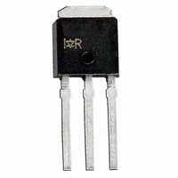
IRLU8113PBF International Rectifier, IRLU8113PBF Datasheet - Page 6

IRLU8113PBF
Manufacturer Part Number
IRLU8113PBF
Description
MOSFET N-CH 30V 94A I-PAK
Manufacturer
International Rectifier
Series
HEXFET®r
Datasheet
1.IRLR8113TRPBF.pdf
(12 pages)
Specifications of IRLU8113PBF
Fet Type
MOSFET N-Channel, Metal Oxide
Fet Feature
Logic Level Gate
Rds On (max) @ Id, Vgs
6 mOhm @ 15A, 10V
Drain To Source Voltage (vdss)
30V
Current - Continuous Drain (id) @ 25° C
94A
Vgs(th) (max) @ Id
2.25V @ 250µA
Gate Charge (qg) @ Vgs
32nC @ 4.5V
Input Capacitance (ciss) @ Vds
2920pF @ 15V
Power - Max
89W
Mounting Type
Through Hole
Package / Case
IPak, TO-251, DPak, VPak (3 straight leads + tab)
Transistor Polarity
N-Channel
Resistance Drain-source Rds (on)
7.4 mOhms
Drain-source Breakdown Voltage
30 V
Gate-source Breakdown Voltage
20 V
Continuous Drain Current
94 A
Power Dissipation
89 W
Mounting Style
SMD/SMT
Gate Charge Qg
22 nC
Lead Free Status / RoHS Status
Lead free / RoHS Compliant
Other names
*IRLU8113PBF
Available stocks
Company
Part Number
Manufacturer
Quantity
Price
Company:
Part Number:
IRLU8113PBF
Manufacturer:
INF
Quantity:
3 939
Fig 12a. Unclamped Inductive Test Circuit
6
Fig 12b. Unclamped Inductive Waveforms
Fig 13. Gate Charge Test Circuit
I
AS
12V
V
GS
R G
20V
Same Type as D.U.T.
V
V DS
GS
Current Regulator
.2µF
t p
50KΩ
3mA
I AS
Current Sampling Resistors
D.U.T
t p
.3µF
0.01 Ω
L
I
G
D.U.T.
15V
I
V
D
(BR)DSS
DRIVER
+
-
V
+
-
DS
V DD
A
Fig 14b. Switching Time Waveforms
Fig 14a. Switching Time Test Circuit
700
600
500
400
300
200
100
V
90%
10%
V
0
DS
GS
Fig 12c. Maximum Avalanche Energy
25
Starting T J , Junction Temperature (°C)
t
d(on)
Duty Factor < 0.1%
Pulse Width < 1µs
V
50
GS
Vs. Drain Current
t
r
V
DS
75
100
D.U.T
L
D
t
d(off)
V
TOP
BOTTOM 13A
125
DD
www.irf.com
t
f
150
I D
8.3A
9.4A
175


