TPCF8B01(TE85L,F) Toshiba, TPCF8B01(TE85L,F) Datasheet
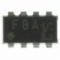
MOSFET P-CH 20V 2.7A VS-8

TPCF8B01(TE85L,F)

Manufacturer Part Number
TPCF8B01(TE85L,F)
Description
MOSFET P-CH 20V 2.7A VS-8
Manufacturer
Toshiba
Datasheet

Specifications of TPCF8B01(TE85L,F)

Fet Type
MOSFET P-Channel, Metal Oxide
Fet Feature
Diode (Isolated)
Rds On (max) @ Id, Vgs
110 mOhm @ 1.4A, 4.5V
Drain To Source Voltage (vdss)
20V
Current - Continuous Drain (id) @ 25° C
2.7A
Vgs(th) (max) @ Id
1.2V @ 200µA
Gate Charge (qg) @ Vgs
6nC @ 5V
Input Capacitance (ciss) @ Vds
470pF @ 10V
Power - Max
1.35W
Mounting Type
Surface Mount
Package / Case
*
Configuration
Single Dual Drain
Transistor Polarity
P-Channel
Resistance Drain-source Rds (on)
0.11 Ohms
Drain-source Breakdown Voltage
- 20 V
Gate-source Breakdown Voltage
8 V
Continuous Drain Current
2.7 A
Power Dissipation
1.35 W
Mounting Style
SMD/SMT
Lead Free Status / RoHS Status
Lead free / RoHS Compliant
Other names
TPCF8B01(TE85L,F)
TPCF8B01FTR
Notebook PC Applications
Portable Equipment Applications
Absolute Maximum Ratings
MOSFET
SBD
Absolute Maximum Ratings for MOSFET and SBD
Low drain-source ON resistance: R
High forward transfer admittance: |Y
Low leakage current: I
Enhancement-model: V
Low forward voltage: V
Drain-source voltage
Drain-gate voltage (R
Gate-source voltage
Drain current
Single pulse avalanche energy
Avalanche current
Repetitive avalanche energy
Single-device value at dual operation
Repetitive peak reverse voltage
Average forward current (Note 2a, 6)
Peak one cycle surge forward current
(non-repetitive)
Drain power
dissipation
(t = 5 s) (Note 2a) Single-device value at
Drain power
dissipation
(t = 5 s) (Note 2b) Single-device value at
Channel temperature
Storage temperature range
Note: For (Note 1), (Note 2), (Note 3), (Note 4), (Note 5), (Note 6) and (Note 7), please refer to the next page.
TOSHIBA Multi-Chip Device Silicon P Channel MOS Type (U-MOS III) / Schottky Barrier Diode
(Ta = 25°C)
Using continuously under heavy loads (e.g. the application of high temperature/current/voltage and the significant change in
temperature, etc.) may cause this product to decrease in the reliability significantly even if the operating conditions (i.e.
operating temperature/current/voltage, etc.) are within the absolute maximum ratings. Please design the appropriate
reliability upon reviewing the Toshiba Semiconductor Reliability Handbook (“Handling Precautions”/Derating Concept and
Methods) and individual reliability data (i.e. reliability test report and estimated failure rate, etc).
(Ta = 25°C)
Characteristics
Characteristics
Characteristics
DC
Pulse
Single-device operation
dual operation (Note 3b)
Single-device operation
dual operation (Note 3b)
GS
= 20 kΩ)
DSS
FM(2)
th
(Note 2a, 3b, 5)
= -0.5 to-1.2 V(V
=-10 µA (max) (V
= 0.46V(typ.)
(Note 3a)
(Note 3a)
(Note 1)
(Note 1)
(Note 4)
DS (ON)
TPCF8B01
fs
| = 4.7 S (typ.)
Symbol
Symbol
Symbol
V
DS
V
V
I
P
P
P
P
V
I
E
F(AV)
= 72 mΩ (typ.)
E
T
FSM
T
I
I
DGR
RRM
D (1)
D (2)
D (1)
D (2)
DSS
GSS
I
DP
AR
DS
AS
AR
stg
D
ch
=-10 V, I
= -20 V)
-55~150
7(50Hz)
1
Rating
Rating
Rating
D
-10.8
-1.35
0.11
1.35
1.12
0.53
0.33
-2.7
150
-20
-20
1.2
1.0
±8
20
= -200 µA)
(Ta = 25°C)
Unit
Unit
Unit
mJ
mJ
°C
°C
W
V
V
V
A
A
V
A
A
Weight: 0.011 g (typ.)
Circuit Configuration
JEDEC
JEITA
TOSHIBA
1
8
7
2
TPCF8B01
2-3U1C
2006-11-16
6
3
Unit: mm
5
4

Related parts for TPCF8B01(TE85L,F)

TPCF8B01(TE85L,F) Summary of contents

Page 1

... TOSHIBA Multi-Chip Device Silicon P Channel MOS Type (U-MOS III) / Schottky Barrier Diode Notebook PC Applications Portable Equipment Applications • Low drain-source ON resistance: R • High forward transfer admittance: |Y • Low leakage current: I =-10 µA (max) (V DSS • Enhancement-model -0.5 to-1.2 V(V th • Low forward voltage ...

Page 2

Thermal Characteristics for MOSFET and SBD Characteristics Single-device operation Thermal resistance, (Note 3a) channel to ambient ( (Note 2a) Single-device value at dual operation (Note 3b) Single-device operation Thermal resistance, (Note 3a) channel to ambient (t = ...

Page 3

Electrical Characteristics MOSFET Characteristics Gate leakage current Drain cut-off current Drain-source breakdown voltage Gate threshold voltage Drain-source ON resistance Forward transfer admittance Input capacitance Reverse transfer capacitance Output capacitance Rise time Turn-on time Switching time Fall time ...

Page 4

MOSFET I – −5 −2.5 −4 −4.5 −2.8 −4 −5 −3 −3.5 −3 −2 −1 Common source Ta = 25°C Pulse test 0 −0.2 −0.4 −0.6 0 Drain-source voltage – −5 ...

Page 5

R – (ON) 300 Common source −1.4 A Pulse test 250 −0 −1.8 V 200 −1 −2.7 A 150 −0.7 A 100 −2.5 V ...

Page 6

Single pulse 100 100 m Safe operating area 100 I D max (pulse ms* 10 ms* 1 ※ Single pulse Ta=25℃ Curves must be derated linearly with increase in temperature. V ...

Page 7

SBD i – Tj=150℃ 1 125℃ 75℃ 25℃ 0.1 0.01 0.8 0.0 0.2 0.4 0.6 Instantaneous forward voltage v F (V) Ta max – (AV) Device mounted on a glass-epoxy board(a) (Note 2a) 160 ...

Page 8

I – Pulse test 1 0.1 V =20V R 0.01 10V 5V 0.001 0.0001 100 120 Junction temperature T j (°C) (typ.) 0.06 Rectangular waveform 0° 360° 0. α ...

Page 9

... The information contained herein is presented only as a guide for the applications of our products. No responsibility is assumed by TOSHIBA for any infringements of patents or other rights of the third parties which may result from its use. No license is granted by implication or otherwise under any patent or patent rights of TOSHIBA or others. • ...

Related keywords