IRF7324D1TRPBF International Rectifier, IRF7324D1TRPBF Datasheet
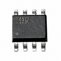
MOSFET P-CH 20V 2.2A 8-SOIC

IRF7324D1TRPBF

Manufacturer Part Number
IRF7324D1TRPBF
Description
MOSFET P-CH 20V 2.2A 8-SOIC
Manufacturer
International Rectifier
Series
FETKY™r
Datasheet

Specifications of IRF7324D1TRPBF

Fet Type
MOSFET P-Channel, Metal Oxide
Fet Feature
Diode (Isolated)
Rds On (max) @ Id, Vgs
270 mOhm @ 1.2A, 4.5V
Drain To Source Voltage (vdss)
20V
Current - Continuous Drain (id) @ 25° C
2.2A
Vgs(th) (max) @ Id
700mV @ 250µA
Gate Charge (qg) @ Vgs
7.8nC @ 4.5V
Input Capacitance (ciss) @ Vds
260pF @ 15V
Power - Max
2W
Mounting Type
Surface Mount
Package / Case
8-SOIC (3.9mm Width)
Transistor Polarity
P-Channel
Resistance Drain-source Rds (on)
270 mOhms
Drain-source Breakdown Voltage
- 20 V
Gate-source Breakdown Voltage
12 V
Continuous Drain Current
- 2.2 A
Power Dissipation
2 W
Mounting Style
SMD/SMT
Gate Charge Qg
5.2 nC
Lead Free Status / RoHS Status
Lead free / RoHS Compliant
Other names
IRF7324D1PBFTR
IRF7324D1TRPBF
IRF7324D1TRPBFTR

Available stocks

Company
Part Number
Manufacturer
Quantity
Price
Part Number:
IRF7324D1TRPBF
Manufacturer:
International Rectifier
Quantity:
25 612
l
l
l
l
l
Description
The FETKY
the designer an innovative board space saving solution for switching regulator
applications. Generation 5 HEXFETs utilize advanced processing techniques
to achieve extremely low on-resistance per silicon area. Combining this
technology with International Rectifier's low forward drop Schottky rectifiers
results in an extremely efficient device suitable for use in a wide variety of
portable electronics applications.
The SO-8 has been modified through a customized leadframe for enhanced
thermal characteristics. The SO-8 package is designed for vapor phase,
infrared or wave soldering techniques.
Notes  through … are on page 8
www.irf.com
V
V
I
I
I
P
P
dV/dt
T
T
R
R
Absolute Maximum Ratings
Thermal Resistance
D
D
DM
J
STG
DS
GS
D
D
θJL
θJA
@ T
@ T
Co-packaged HEXFET® Power
MOSFET and Schottky Diode
Ideal for Mobile Phone Applications
Generation V Technology
SO-8 Footprint
Lead-Free
@T
@T
A
A
A
A
= 25°C
= 70°C
= 25°C
= 70°C
TM
family of co-packaged HEXFETs and Schottky diodes offer
Drain-to-Source Voltage
Gate-to-Source Voltage
Continuous Drain Current, V
Pulsed Drain Current
Power Dissipation
Power Dissipation
Peak Diode Recovery
Linear Derating Factor
Operating Junction and
Storage Temperature Range
Junction-to-Drain Lead
Junction-to-Ambient
Parameter
Parameter
f
f
fg
d
g
GS
GS
@ 10V
@ 10V
G
A
S
A
FETKY
1
2
3
4
Top View
Typ.
IRF7324D1PbF
–––
–––
ä
-55 to + 150
MOSFET / Schottky Diode
8
7
6
5
Max.
-0.74
± 12
-2.2
-1.8
-20
-22
2.0
1.3
16
K
K
D
D
Max.
62.5
Schottky Vf = 0.39V
20
R
DS(on)
V
DSS
SO-8
PD-95309A
= -20V
= 0.27Ω
mW/°C
Units
Units
°C/W
V/ns
°C
W
V
A
12/06/04
1

Related parts for IRF7324D1TRPBF

IRF7324D1TRPBF Summary of contents

Page 1

... Generation 5 HEXFETs utilize advanced processing techniques to achieve extremely low on-resistance per silicon area. Combining this technology with International Rectifier's low forward drop Schottky rectifiers results in an extremely efficient device suitable for use in a wide variety of portable electronics applications. ...

Page 2

IRF7324D1PbF MOSFET Electrical Characteristics @ T Parameter BV Drain-to-Source Breakdown Voltage DSS R Static Drain-to-Source On-Resistance DS(on) V Gate Threshold Voltage GS(th) I Drain-to-Source Leakage Current DSS I Gate-to-Source Forward Leakage GSS Gate-to-Source Reverse Leakage gfs Forward Transconductance Q Total ...

Page 3

VGS TOP -7.5V -5.0V -4.0V 100 -3.5V -3.0V -2.5V -2.0V BOTTOM -1. -1.5V 0.1 ≤ 60µs PULSE WIDTH Tj = 25°C 0.01 0 Drain-to-Source Voltage (V) 100.0 10.0 1 -10V ...

Page 4

IRF7324D1PbF 1 -2. -4.5V 1.0 0.5 -60 -40 - Junction Temperature (°C) 0.4 0.3 0.2 0.1 0.0 2.0 4.0 6 Gate-to-Source Voltage (V) Fig ...

Page 5

0V MHZ C iss = SHORTED 500 C rss = oss = 400 Ciss 300 200 Coss ...

Page 6

IRF7324D1PbF Schottky Diode Characteristics 10 1 0.1 0.0 0.2 0.4 0.6 Forward Voltage Drop - V Forward Votage Drop - V Fig. 12 -Typical Forward Voltage Drop Characteristics ...

Page 7

SO-8 (Fetky) Package Outline 0.25 [.010 0.25 [.010 NOT DIMENS IONING & TOLERANCING PER ...

Page 8

IRF7324D1PbF SO-8 (Fetky) Tape and Reel TERMINAL NUMBER 1 8.1 ( .318 ) 7.9 ( .312 ) NOTES: 1. CONTROLLING DIMENSION : MILLIMETER. 2. ALL DIMENSIONS ARE SHOWN IN MILLIMETERS(INCHES). 3. OUTLINE CONFORMS TO EIA-481 & EIA-541. 330.00 (12.992) MAX. ...

Related keywords