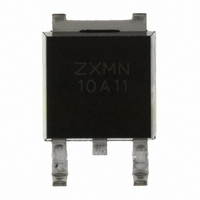
ZXMN10A11K Diodes Zetex, ZXMN10A11K Datasheet - Page 4

ZXMN10A11K
Manufacturer Part Number
ZXMN10A11K
Description
MOSFET N-CHAN 100V DPAK
Manufacturer
Diodes Zetex
Datasheet
1.ZXMN10A11K.pdf
(8 pages)
Specifications of ZXMN10A11K
Fet Type
MOSFET N-Channel, Metal Oxide
Fet Feature
Standard
Rds On (max) @ Id, Vgs
350 mOhm @ 2.6A, 10V
Drain To Source Voltage (vdss)
100V
Current - Continuous Drain (id) @ 25° C
2.4A
Vgs(th) (max) @ Id
4V @ 250µA
Gate Charge (qg) @ Vgs
5.4nC @ 10V
Input Capacitance (ciss) @ Vds
274pF @ 50V
Power - Max
2.11W
Mounting Type
Surface Mount
Package / Case
DPak, TO-252 (2 leads+tab), SC-63
Lead Free Status / RoHS Status
Lead free / RoHS Compliant
Other names
ZXMN10A11KTR
Electrical Characteristics
OFF CHARACTERISTICS
Drain-Source Breakdown Voltage
Zero Gate Voltage Drain Current
Gate-Source Leakage
ON CHARACTERISTICS
Gate Threshold Voltage
Static Drain-Source On-Resistance (Note 7)
Forward Transconductance (Notes 7 & 8)
Diode Forward Voltage (Note 7)
Reverse recovery time (Note 8)
Reverse recovery charge (Note 8)
DYNAMIC CHARACTERISTICS (Note 8)
Input Capacitance
Output Capacitance
Reverse Transfer Capacitance
Total Gate Charge (Note 9)
Total Gate Charge (Note 9)
Gate-Source Charge (Note 9)
Gate-Drain Charge (Note 9)
Turn-On Delay Time (Note 9)
Turn-On Rise Time (Note 9)
Turn-Off Delay Time (Note 9)
Turn-Off Fall Time (Note 9)
Notes:
ZXMN10A11K
Document Number DS32058 Rev. 2 - 2
7. Measured under pulsed conditions. Pulse width ≤ 300μs; duty cycle ≤ 2%
8. For design aid only, not subject to production testing.
9. Switching characteristics are independent of operating junction temperatures.
Characteristic
@T
A
= 25°C unless otherwise specified
Symbol
R
BV
V
DS (ON)
t
t
I
I
C
V
C
C
Q
Q
D(on)
D(off)
GS(th)
DSS
GSS
Q
Q
Q
g
t
oss
t
t
SD
rss
DSS
rr
iss
fs
gs
gd
r
f
rr
g
g
www.diodes.com
Min
100
4 of 8
⎯
⎯
⎯
⎯
⎯
⎯
⎯
⎯
⎯
⎯
⎯
⎯
⎯
⎯
⎯
⎯
⎯
⎯
2
0.850
Typ
274
3.5
5.4
1.4
1.5
2.7
1.7
7.4
3.5
26
30
21
11
⎯
⎯
⎯
⎯
⎯
4
0.350
0.450
0.950
±100
Max
⎯
⎯
⎯
⎯
⎯
⎯
⎯
⎯
⎯
⎯
⎯
⎯
⎯
⎯
⎯
1
4
Diodes Incorporated
A Product Line of
Unit
µA
nA
nC
nC
nC
nC
nC
ns
pF
pF
pF
ns
ns
ns
ns
Ω
V
V
S
V
I
V
V
I
V
V
V
I
I
V
f = 1MHz
V
V
V
I
D
D
S
S
D
DS
GS
GS
GS
DS
DS
GS
GS
DD
= 250μA, V
= 1.85A, V
= 1.0A, di/dt = 100A/μs
= 250μA, V
= 1.0A, R
= 100V, V
= 15V, I
= 50V, V
= 6V
= 10V
= ±20V, V
= 10V, I
= 6V, I
= 50V, V
Test Condition
ZXMN10A11K
D
G
D
D
= 1.3A
GS
GS
GS
GS
DS
≅ 6Ω
= 2.6A
GS
= 2.6A
DS
= 0V
= 0V
= 10V
= 0V
= V
= 0V
= 0V
V
I
© Diodes Incorporated
D
DS
GS
= 2.5A
January 2010
= 50V,


