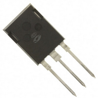
APT5010B2VFRG Microsemi Power Products Group, APT5010B2VFRG Datasheet - Page 2

APT5010B2VFRG
Manufacturer Part Number
APT5010B2VFRG
Description
MOSFET N-CH 500V 47A T-MAX
Manufacturer
Microsemi Power Products Group
Series
POWER MOS V®r
Datasheet
1.APT5010B2VFRG.pdf
(4 pages)
Specifications of APT5010B2VFRG
Fet Type
MOSFET N-Channel, Metal Oxide
Fet Feature
Standard
Rds On (max) @ Id, Vgs
100 mOhm @ 500mA, 10V
Drain To Source Voltage (vdss)
500V
Current - Continuous Drain (id) @ 25° C
47A
Vgs(th) (max) @ Id
4V @ 2.5mA
Gate Charge (qg) @ Vgs
470nC @ 10V
Input Capacitance (ciss) @ Vds
8900pF @ 25V
Power - Max
520W
Mounting Type
Through Hole
Package / Case
T-MAX
Lead Free Status / RoHS Status
Lead free / RoHS Compliant
DYNAMIC CHARACTERISTICS
SOURCE-DRAIN DIODE RATINGS AND CHARACTERISTICS
THERMAL CHARACTERISTICS
1
2
3
Symbol
Symbol
Symbol
Repetitive Rating: Pulse width limited by maximum junction
temperature.
Pulse Test: Pulse width < 380 S, Duty Cycle < 2%
See MIL-STD-750 Method 3471
APT Reserves the right to change, without notice, the specifications and information contained herein.
t
t
I
R
R
C
C
d
d
V
dv
C
Q
Q
RRM
I
Q
Q
(on)
(off)
t
SM
t
I
t
oss
SD
rss
iss
S
rr
gs
gd
/
r
f
JC
JA
g
rr
dt
0.005
0.001
0.05
0.01
0.3
0.1
10
Characteristic
Input Capacitance
Output Capacitance
Reverse Transfer Capacitance
Total Gate Charge
Gate-Source Charge
Gate-Drain ("Miller") Charge
Turn-on Delay Time
Rise Time
Turn-off Delay Time
Fall Time
Characteristic / Test Conditions
Continuous Source Current (Body Diode)
Pulsed Source Current
Diode Forward Voltage
Peak Diode Recovery
Reverse Recovery Time
(I
Reverse Recovery Charge
(I
Peak Recovery Current
(I
Characteristic
Junction to Case
Junction to Ambient
S
S
S
-5
= -I
= -I
= -I
FIGURE 1, MAXIMUM EFFECTIVE TRANSIENT THERMAL IMPEDANCE, JUNCTION-TO-CASE vs PULSE DURATION
D
D
D
D=0.5
[Cont.],
[Cont.],
[Cont.],
0.02
0.01
0.05
0.2
0.1
10
di
di
di
/
/
/
-4
dt
dt
dt
3
= 100A/ s)
= 100A/ s)
= 100A/ s)
SINGLE PULSE
dv
1
2
/
dt
(Body Diode)
(V
6
GS
RECTANGULAR PULSE DURATION (SECONDS)
= 0V, I
10
-3
S
= -I
D
[Cont.])
I
I
10
D
D
4
5
6
Test Conditions
= I
= I
-2
V
V
Starting T
These dimensions are equal to the TO-247 without mounting hole
I
V
DD
DD
S
D
D
R
V
V
V
R
f = 1 MHz
V
[Cont.] @ 25 C
[Cont.] @ 25 C
DS
GS
GS
= 200V.
G
GS
= 0.5 V
= 0.5 V
-I
T
T
T
T
T
T
D
= 0.6
j
j
j
j
j
j
= 25V
= 10V
= 15V
= 25 C
= 125 C
= 25 C
= 125 C
= 25 C
= 125 C
= 0V
[Cont.],
j
= +25 C, L = 2.26mH, R
DSS
DSS
10
di
-1
/
dt
= 100A/ s, V
Note:
Peak T J = P DM x Z JC + T C
MIN
MIN
MIN
Duty Factor D =
1.0
DD
t 1
G
= 25 , Peak I
t 2
V
7400
1000
TYP
TYP
TYP
380
312
127
1.6
5.5
DSS
15
27
50
14
16
54
5
t 1
, T
/ t 2
j
APT5010B2VFR
150 C, R
8900
1400
MAX
MAX
MAX
0.24
188
250
500
570
470
190
1.3
L
47
75
30
32
80
10
40
5
= 47A
10
G
Amps
Amps
= 2.0 ,
UNIT
UNIT
Volts
V/ns
UNIT
nC
pF
C/W
ns
ns
C


