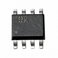
IRF7233PBF International Rectifier, IRF7233PBF Datasheet

IRF7233PBF
Specifications of IRF7233PBF
Available stocks
Related parts for IRF7233PBF
IRF7233PBF Summary of contents
Page 1
... 70°C Power Dissipation D A Linear Derating Factor E Single Pulse Avalanche Energy„ Gate-to-Source Voltage Junction and Storage Temperature Range J, STG Thermal Resistance Parameter R Maximum Junction-to-Ambient θJA www.irf.com IRF7233PbF HEXFET Top View Max. @ -4.5V ±9 -4.5V ±6.0 GS 0.02 - 150 Max. ƒ ® ...
Page 2
... IRF7233PbF Electrical Characteristics @ T Parameter V Drain-to-Source Breakdown Voltage (BR)DSS V Drain-to-Source Breakdown Voltage (BR)DSS Breakdown Voltage Temp. Coefficient ∆V /∆T (BR)DSS J R Static Drain-to-Source On-Resistance DS(on) V Gate Threshold Voltage GS(th) g Forward Transconductance fs I Drain-to-Source Leakage Current DSS Gate-to-Source Forward Leakage GSS Gate-to-Source Reverse Leakage ...
Page 3
... BOTTOM - 1. Fig 2. Typical Output Characteristics 2 1 150°C J 1.0 0.5 = -10V 0.0 A -60 -40 -20 2.5 3.0 Fig 4. Normalized On-Resistance IRF7233PbF VGS - 7.5V - 5.0V - 4.0V - 3.5V - 3.0V - 2.5V - 2.0V 20µs PULSE WIDTH -1. 150° Drain-to-Source Voltage (V) DS -9. -4. 100 120 140 160 ° ...
Page 4
... IRF7233PbF 6000 1kHz iss rss oss ds gd 5000 C iss 4000 3000 C oss C rss 2000 Drain-to-Source Voltage (V) DS Fig 5. Typical Capacitance Vs. Drain-to-Source Voltage 100 T = 150° 25° 0.0 1 Source-to-Drain Voltage (V) SD Fig 7. Typical Source-Drain Diode Forward Voltage SHORTED Fig 6. Typical Gate Charge Vs. ...
Page 5
... Fig 11. Maximum Effective Transient Thermal Impedance, Junction-to-Ambient www.irf.com 140 120 100 125 150 25 ° Starting T , Junction Temperature ( C) Fig 10. Maximum Avalanche Energy Notes: 1. Duty factor Peak 0.001 0. Rectangular Pulse Duration (sec) 1 IRF7233PbF I D TOP -4.2A -7.6A BOTTOM -9. 100 125 ° J Vs. Drain Current ...
Page 6
... IRF7233PbF SO-8 Package Outline Dimensions are shown in milimeters (inches 0.25 [.010 NOT DIMENS IONING & T OLERANCING PER AS ME Y14.5M-1994. 2. CONT ROLLING DIMENS ION: MILLIMET ER 3. DIMENS IONS ARE S HOWN IN MILLIMET ERS [INCHES ]. 4. OUT LINE CONFORMS T O JEDEC OUT LINE MS -012AA. 5 DIMENS ION DOES NOT INCLUDE MOLD PROT RUS IONS. ...
Page 7
... FEED DIRECTION 7.9 ( .312 ) 330.00 (12.992) MAX. Data and specifications subject to change without notice. Qualifications Standards can be found on IR’s Web site. Visit us at www.irf.com for sales contact information.11/04 IRF7233PbF 12.3 ( .484 ) 11.7 ( .461 ) 14.40 ( .566 ) 12.40 ( .488 ) TAC Fax: (310) 252-7903 7 ...


