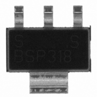
BSP318S L6327 Infineon Technologies, BSP318S L6327 Datasheet
Home Discrete Semiconductor Products MOSFETs, GaNFETs - Single BSP318S L6327
Manufacturer Part Number
BSP318S L6327
Description
MOSFET N-CH 60V 2.6A SOT-223
Manufacturer
Infineon Technologies
Specifications of BSP318S L6327
Package / Case
SOT-223 (3 leads + Tab), SC-73, TO-261
Fet Type
MOSFET N-Channel, Metal Oxide
Fet Feature
Logic Level Gate
Rds On (max) @ Id, Vgs
90 mOhm @ 2.6A, 10V
Drain To Source Voltage (vdss)
60V
Current - Continuous Drain (id) @ 25° C
2.6A
Vgs(th) (max) @ Id
2V @ 20µA
Gate Charge (qg) @ Vgs
20nC @ 10V
Input Capacitance (ciss) @ Vds
380pF @ 25V
Power - Max
1.8W
Mounting Type
Surface Mount
Minimum Operating Temperature
- 55 C
Configuration
Single Dual Drain
Transistor Polarity
N-Channel
Resistance Drain-source Rds (on)
0.09 Ohm @ 10 V
Drain-source Breakdown Voltage
60 V
Gate-source Breakdown Voltage
+/- 20 V
Continuous Drain Current
2.6 A
Power Dissipation
1800 mW
Maximum Operating Temperature
+ 150 C
Mounting Style
SMD/SMT
Lead Free Status / RoHS Status
Lead free / RoHS Compliant
Lead Free Status / RoHS Status
Lead free / RoHS Compliant, Lead free / RoHS Compliant
Other names
BSP318SL6327INTR
Type
BSP318S
SIPMOS
Features
Maximum Ratings,at T
Parameter
Continuous drain current
Pulsed drain current
T
Avalanche energy, single pulse
I
Avalanche current,periodic limited by T
Avalanche energy, periodic limited by T
Reverse diode d v /d t
I
T
Gate source voltage
Power dissipation
T
Operating and storage temperature
IEC climatic category; DIN IEC 68-1
•
• Qualified according to AEC Q101
D
S
Enhancement mode
A
jmax
A
N-Channel
Avalanche rated
Logic Level
d v /d t rated
Pb-free lead plating; RoHS compliant
= 2.6 A, V
= 2.6 A, V
= 25 °C
= 25 °C
= 150 °C
DS
DD
Small-Signal-Transistor
= 20 V, d i /d t = 200 A/µs,
= 25 V, R
Package
PG-SOT223
j
= 25 °C, unless otherwise specified
GS
= 25
Tape and Reel
L6327: 1000 pcs/r
Product Summary
Drain source voltage
Drain-Source on-state resistance R
Continuous drain current
jmax
jmax
Rev 2.2
Page 1
Pin 1
G
Symbol
I
I
E
I
E
d v /d t
V
P
T
Pin 2, 4
D
D puls
AR
j ,
AS
AR
GS
tot
Marking
BSP318S
T
D
stg
PIN 3
S
-55... +150
55/150/56
Non dry
V
I
Packaging
Value
D
10.4
0.18
DS
DS(on)
2.6
2.6
1.8
60
20
6
4
2008-03-21
BSP318S
0.09
2.6
60
1
Unit
A
mJ
A
mJ
kV/µs
V
W
°C
V
A
2
VPS05163
3
Related parts for BSP318S L6327
BSP318S L6327 Summary of contents
SIPMOS Small-Signal-Transistor Features N-Channel Enhancement mode Avalanche rated Logic Level rated • Pb-free lead plating; RoHS compliant • Qualified according to AEC Q101 Type Package BSP318S PG-SOT223 Maximum Ratings, Parameter Continuous drain current Pulsed ...
Thermal Characteristics Parameter Characteristics Thermal resistance, junction - soldering point (Pin 4) SMD version, device on PCB: @ min. footprint cooling area Electrical Characteristics Parameter Static Characteristics Drain- source breakdown voltage V = ...
Electrical Characteristics Parameter Dynamic Characteristics Transconductance DS(on)max D Input capacitance MHz GS DS Output capacitance ...
Electrical Characteristics Parameter Dynamic Characteristics Gate charge at threshold 0 Gate charge 2.6 ...
Power Dissipation tot A BSP318S 1.9 W 1.6 1.4 1.2 1.0 0.8 0.6 0.4 0.2 0 Safe operating area parameter : D ...
Typ. output characteristic =25° parameter µs p BSP318S 6 1.80W tot 5 5.0 4.5 4.0 ...
Typ. capacitances parameter MHz Avalanche Energy AS parameter 2 ...
Drain-source breakdown voltage (BR)DSS j BSP318S -60 - Rev 2.2 °C 100 180 T j Page 8 BSP318S 2008-03-21 ...
Rev 2.2 Page 9 BSP318S 2008-03-21 ...
Related keywords
bsp31 bsp315p bsp315 bsp317p bsp316 bsp318s BSP318S L6327 datasheet BSP318S L6327 data sheet BSP318S L6327 pdf datasheet BSP318S L6327 component BSP318S L6327 part BSP318S L6327 distributor BSP318S L6327 RoHS BSP318S L6327 datasheet download


