SPD02N60S5 Infineon Technologies, SPD02N60S5 Datasheet
SPD02N60S5
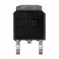
Specifications of SPD02N60S5
SPD02N60S5
SPD02N60S5INTR
SPD02N60S5XT
Available stocks


Related parts for SPD02N60S5

SPD02N60S5 Summary of contents
Page 1
... Operating and storage temperature Rev. 2.5 Ordering Code Q67040-S4226 Q67040-S4213 Symbol puls jmax limited jmax limited jmax tot stg Page 1 SPU02N60S5 SPD02N60S5 600 DS(on) I 1.8 D PG-TO252 PG-TO251 Marking 02N60S5 02N60S5 Value 1.8 1.1 3.2 50 0.07 1.8 ±20 ± -55... +150 2008-04-07 V Ω ...
Page 2
... V =V GS(th =600V, V =0V, V DSS DS GS =25° =150° =20V, V =0V V GSS GS DS =10V, I =1.1A, V DS(on =25° =150° Page 2 SPU02N60S5 SPD02N60S5 Value Unit 20 V/ns Values Unit min. typ. max K 260 °C Values Unit min. typ. max. 600 - - V - 700 - 3.5 4 ...
Page 3
... Symbol Conditions ≥ DS(on)max =1.1A D =0V, V =25V iss f=1MHz oss C rss =350V, V =0/10V d(on =50 Ω I =1.8A d(off =350V, I =1. =350V, I =1.8A 10V =350V, I =1. (plateau) DD Page 3 SPU02N60S5 SPD02N60S5 Values min. typ. max 240 - - 7 2008-04-07 Unit ...
Page 4
... /dt=100A/µ Unit Symbol Thermal capacitance K/W C th1 C th2 C th3 C th4 C th5 C th6 th1 th th1 th2 th,n Page 4 SPU02N60S5 SPD02N60S5 Values min. typ 860 = 1.6 Value typ. 0.00002806 0.0001113 0.0001679 0.000547 0.001388 0.019 E xternal H eatsink T case Unit max. 1.8 A 3.2 1.2 ...
Page 5
... parameter µ Rev. 2.5 2 Safe operating area parameter : 100 120 °C 160 Drain-source on-state resistance R DS(on) parameter : I Ω 20V 12V 10V 9V 8. Page 5 SPU02N60S5 SPD02N60S5 ) DS =25° 0.001 SPU02N60S5 98% 4 typ 2 0 -60 - 100 °C 180 T j 2008-04-07 ...
Page 6
... Rev. 2.5 6 Typ. gate charge = DS(on)max GS parameter Avalanche SOA par 1.6 1.4 1.2 0.8 0.6 0.4 0 Page 6 SPU02N60S5 SPD02N60S5 ) Gate = 1.8 A pulsed D SPU02N60S5 16 0 max 0 max ≤ 150 ° j(START =125°C j(START ...
Page 7
... Avalanche energy par 1. 100 11 Typ. capacitances parameter: V =0V, f=1 MHz iss oss rss Rev. 2.5 10 Drain-source breakdown voltage V (BR)DSS 720 V 680 660 640 620 600 580 560 540 120 °C 160 100 V DS Page 7 SPU02N60S5 SPD02N60S5 = SPU02N60S5 -60 - 100 2008-04-07 °C 180 T j ...
Page 8
... Definition of diodes switching characteristics Rev. 2.5 Page 8 SPU02N60S5 SPD02N60S5 2008-04-07 ...
Page 9
... PG-TO252-3-1, PG-TO252-3-11, PG-TO252-3-21 (D-PAK) Rev. 2.5 Page 9 SPU02N60S5 SPD02N60S5 2008-04-07 ...
Page 10
... PG-TO251-3-1, PG-TO251-3-21 (I-PAK) Rev. 2.5 Page 10 SPU02N60S5 SPD02N60S5 2008-04-07 ...
Page 11
... Rev. 2.5 Page 11 SPU02N60S5 SPD02N60S5 2008-04-07 ...