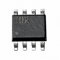
IRF7807TR International Rectifier, IRF7807TR Datasheet - Page 3

IRF7807TR
Manufacturer Part Number
IRF7807TR
Description
MOSFET N-CH 30V 8.3A 8-SOIC
Manufacturer
International Rectifier
Series
HEXFET®r
Datasheet
1.IRF7807.pdf
(8 pages)
Specifications of IRF7807TR
Fet Type
MOSFET N-Channel, Metal Oxide
Fet Feature
Standard
Rds On (max) @ Id, Vgs
25 mOhm @ 7A, 4.5V
Drain To Source Voltage (vdss)
30V
Current - Continuous Drain (id) @ 25° C
8.3A
Vgs(th) (max) @ Id
1V @ 250µA
Gate Charge (qg) @ Vgs
17nC @ 5V
Power - Max
2.5W
Mounting Type
Surface Mount
Package / Case
8-SOIC (3.9mm Width)
Lead Free Status / RoHS Status
Contains lead / RoHS non-compliant
Available stocks
Company
Part Number
Manufacturer
Quantity
Price
Part Number:
IRF7807TR
Manufacturer:
IR
Quantity:
20 000
Part Number:
IRF7807TRPBF
Manufacturer:
IR
Quantity:
20 000
Power MOSFET Selection for DC/DC
Converters
Control FET
in the switching elements of the circuit - Q1 and Q2.
Power losses in the high side switch Q1, also called the
Control FET, are impacted by the R
but these conduction losses are only about one half of
the total losses.
P
and Q
that is included in all MOSFET data sheets. The impor-
tance of splitting this gate-source charge into two sub
elements, Q
the gate driver between the time that the threshold volt-
age has been reached (t1) and the time the drain cur-
rent rises to I
begins to change. Minimizing Q
reducing switching losses in Q1.
capacitance of the MOSFET during every switching
cycle. Figure 2 shows how Q
lel combination of the voltage dependant (non-linear)
capacitance’s C
supply input buss voltage.
www.irf.com
P
loss
loss
Special attention has been given to the power losses
Power losses in the control switch Q1 are given by;
This can be expanded and approximated by;
This simplified loss equation includes the terms Q
Q
Q
Q
gs2
gs2
oss
= P
oss
is a sub element of traditional gate-source charge
is the charge that must be supplied to the output
indicates the charge that must be supplied by
I
Q
which are new to Power MOSFET data sheets.
I
Q
rms
conduction
g
2
oss
2
gs1
Q
dmax
i
V
g
gd
and Q
g
ds
R
V
ds(on)
in
and C
(t2) at which time the drain voltage
+ P
V
f
gs2
in
f
switching
, can be seen from Fig 1.
dg
when multiplied by the power
f
oss
+ P
is formed by the paral-
gs2
I
ds(on)
drive
is a critical factor in
Q
+ P
i
of the MOSFET,
gs2
g
output
V
in
f
gs2
Figure 1: Typical MOSFET switching waveform
Synchronous FET
by;
*dissipated primarily in Q1.
P
P
loss
loss
The power loss equation for Q2 is approximated
t0
V
GTH
P
I
conduction
IRF7807/IRF7807A
Q
rms
Q
t1
g
2
oss
2
V
t2
R
g
V
ds(on)
in
P
Drain Current
drive
f
t3
f
P
output
*
Drain Voltage
Q
rr
Gate Voltage
V
in
4
1
2
f
3


