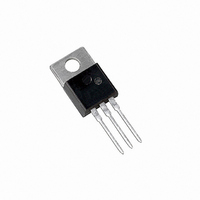
NTP75N03L09G ON Semiconductor, NTP75N03L09G Datasheet - Page 3

NTP75N03L09G
Manufacturer Part Number
NTP75N03L09G
Description
MOSFET N-CH 30V 75A TO220AB
Manufacturer
ON Semiconductor
Datasheet
1.NTB75N03L09T4G.pdf
(8 pages)
Specifications of NTP75N03L09G
Fet Type
MOSFET N-Channel, Metal Oxide
Fet Feature
Logic Level Gate
Rds On (max) @ Id, Vgs
8 mOhm @ 37.5A, 5V
Drain To Source Voltage (vdss)
30V
Current - Continuous Drain (id) @ 25° C
75A
Vgs(th) (max) @ Id
2V @ 250µA
Gate Charge (qg) @ Vgs
75nC @ 5V
Input Capacitance (ciss) @ Vds
5635pF @ 25V
Power - Max
2.5W
Mounting Type
Through Hole
Package / Case
TO-220-3 (Straight Leads)
Lead Free Status / RoHS Status
Lead free / RoHS Compliant
Other names
NTP75N03L09GOS
Available stocks
Company
Part Number
Manufacturer
Quantity
Price
Company:
Part Number:
NTP75N03L09G
Manufacturer:
ON
Quantity:
12 500
2. Pulse Test: Pulse Width v 300 mS, Duty Cycle v 2%.
3. Switching characteristics are independent of operating junction temperatures.
4. From characterization test data.
ELECTRICAL CHARACTERISTICS
OFF CHARACTERISTICS
ON CHARACTERISTICS (Note 2)
DYNAMIC CHARACTERISTICS (Note 4)
SWITCHING CHARACTERISTICS (Notes 3 & 4)
SOURCE−DRAIN DIODE CHARACTERISTICS
Input Capacitance
Output Capacitance
Transfer Capacitance
Turn−On Delay Time
Rise Time
Turn−Off Delay Time
Fall Time
Gate Charge
Forward On−Voltage
Reverse Recovery Time
(Note 4)
Reverse Recovery Stored
Charge (Note 4)
Drain −Source Breakdown Voltage (Note 2)
Temperature Coefficient (Negative)
Zero Gate Voltage Drain Current
Gate−Body Leakage Current
Gate Threshold Voltage (Note 2)
Threshold Temperature Coefficient (Negative)
Static Drain−to−Source On−Resistance (Note 2)
Static Drain−to−Source On Resistance (Note 2)
Forward Transconductance (Notes 2 & 4)
(V
(V
(V
(V
(V
(V
(V
GS
DS
DS
DS
GS
GS
GS
= 30 Vdc, V
= 30 Vdc, V
= V
= 0 Vdc, I
= 5.0 Vdc, I
= 10 Vdc, I
= 10 Vdc, I
GS
, I
D
D
= 250 mAdc)
D
D
= 250 mAdc)
D
GS
GS
= 75 Adc)
= 37.5 Adc, T
= 37.5 Adc)
= 0 Vdc)
= 0 Vdc, T
Characteristic
J
J
= 150°C)
= 125°C)
(I
S
= 75 Adc, V
(T
V
A
(I
dl
(I
(V
DD
S
= 25°C unless otherwise noted)
V
S
S
NTP75N03L09, NTB75N03L09
R
= 75 Adc, V
/dt = 100 A/ms) (Note 2)
DS
DS
= 75 Adc, V
= 20 Vdc, I
G
(V
(V
= 24 Vdc) (Note 2)
= 25 Vdc, V
(V
= 4.7 W) (Note 2)
f = 1.0 MHz)
I
GS
GS
D
GS
GS
(Note 2)
= 75 Adc,
(V
= 5.0 Vdc,
= 5.0 Vdc,
= 0 Vdc, T
= ±20 Vdc, V
DS
http://onsemi.com
GS
D
GS
= 3 Vdc, I
= 75 Adc,
= 0 Vdc)
GS
= 0 Vdc
= 0,
J
3
= 125°C)
DS
D
= 20 Adc)
= 0 Vdc)
V
Symbol
R
V
V
(BR)DSS
t
t
I
C
I
DS(on)
DS(on)
Q
GS(th)
C
C
V
g
d(on)
d(off)
DSS
GSS
Q
Q
Q
t
t
t
FS
oss
t
t
rss
SD
RR
iss
rr
a
b
r
f
T
1
2
Min
1.0
30
−
−
−
−
−
−
−
−
−
−
−
−
−
−
−
−
−
−
−
−
−
−
−
−
0.023
4398
1160
0.52
0.35
1.19
1.09
Typ
−57
317
130
105
1.6
6.5
34
−6
58
16
65
57
11
34
37
20
17
−
−
−
±100
5635
1894
Max
0.68
0.50
1.25
430
200
175
110
1.0
2.0
8.0
10
30
75
15
50
−
−
−
−
−
−
−
−
−
mV°C
mV°C
mAdc
nAdc
Unit
Vdc
Vdc
Vdc
Vdc
mW
mW
nC
mC
pF
ns
ns


