BSC106N025S G Infineon Technologies, BSC106N025S G Datasheet
BSC106N025S G
Specifications of BSC106N025S G
SP000095470


Related parts for BSC106N025S G

BSC106N025S G Summary of contents
Page 1
... Symbol Conditions I T =25 ° =100 ° =25 ° =45 K/W thJA =25 °C D,pulse C =25 Ω = = = /dt di /dt =200 A/µs, T =150 °C j,max =25 °C tot C T =25 ° =45 K/W thJA stg page 1 BSC106N025S 10.6 mΩ PG-TDSON-8 Value Unit 120 kV/µs ± 2.8 -55 ... 150 °C 55/150/56 2009-11-03 ...
Page 2
... GS(th = DSS T =25 ° = =125 ° = GSS =4 =15 A DS( |>2 DS(on)max = (one layer, 70 µm thick) copper area for drain page 2 BSC106N025S G Values Unit min. typ. max 2.4 K 1.2 1 0.1 1 µ 100 - 10 100 nA - 13.4 16.7 mΩ - 8.8 10.6 Ω 2009-11-03 ...
Page 3
... DD GS =2.7 Ω d(off g( plateau V =0 g(sync = oss =25 ° S,pulse = =25 ° = /dt =400 A/µs F page 3 BSC106N025S G Values Unit min. typ. max. - 1030 1370 pF - 396 527 - 3.9 5 3.8 5 3.0 4.5 - 3.7 4 1.6 2.2 - 2.5 3.8 - 4.6 6 120 - 0.93 1 2009-11-03 ...
Page 4
... V Rev. 1.4 2 Drain current I =f 120 160 0 [° Max. transient thermal impedance Z =f(t thJC p parameter µ µs 100 µ [V] DS page 4 BSC106N025S G ≥ 120 T [° 0.5 0.2 0.1 0.05 0.02 0.01 single pulse - [s] p 160 0 10 2009-11-03 ...
Page 5
... Typ. output characteristics I =f =25 ° parameter 4 Typ. transfer characteristics I =f |>2 DS(on)max parameter 150 ° Rev. 1.4 6 Typ. drain-source on resistance R =f(I DS(on) parameter 3 3 Typ. forward transconductance g =f ° [V] GS page 5 BSC106N025S =25 ° 3 [A] D =25 ° [ 2009-11-03 ...
Page 6
... Typ. gate threshold voltage V =f(T GS(th) parameter: I 2.4 2 1.6 1.2 typ 0.8 0 140 190 -60 [° Forward characteristics of reverse diode I =f parameter Crss [V] DS page 6 BSC106N025S 200 µA 20 µA - 140 T [° °C, 98% 25 °C 150 °C, 98% 150 °C 0 0.5 1 1.5 V [V] SD 190 2 2009-11-03 ...
Page 7
... I =f parameter: T j(start) 100 Drain-source breakdown voltage V =f BR(DSS -60 - Rev. 1.4 14 Typ. gate charge V =f(Q GS parameter °C 8 100 °C 125 ° 100 1000 [µ Gate charge waveforms s(th) Q g(th) 90 140 190 [°C] j page 7 BSC106N025S =25 A pulsed gate [nC] gate ate 2009-11-03 ...
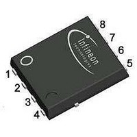
Page 8
... Package Outline P-TDSON-8: Outline Rev. 1.4 PG-TDSON-8 page 8 BSC106N025S G 2009-11-03 ...
Page 9
... Package Outline P-TDSON-8: Tape Dimensions in mm Rev. 1.4 page 9 BSC106N025S G 2009-11-03 ...
Page 10
... Life support devices or systems are intended to be implanted in the human body or to support and/or maintain and sustain and/or protect human life. If they fail reasonable to assume that the health of the user or other persons may be endangered. Rev. 1.4 page 10 BSC106N025S G 2009-11-03 ...