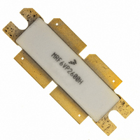
MRF6VP2600HR5 Freescale Semiconductor, MRF6VP2600HR5 Datasheet
MRF6VP2600HR5
Specifications of MRF6VP2600HR5
Available stocks


Related parts for MRF6VP2600HR5

MRF6VP2600HR5 Summary of contents
Page 1
... MTTF calculator available at http://www.freescale.com/rf. Select Software & Tools/Development Tools/Calculators to access MTTF calculators by product. 3. Refer to AN1955, Thermal Measurement Methodology of RF Power Amplifiers http://www.freescale.com/rf. Select Documentation/Application Notes -- AN1955. © Freescale Semiconductor, Inc., 2008--2010. All rights reserved. RF Device Data Freescale Semiconductor = 50 Volts, I ...
Page 2
... W Avg 225 MHz, DVB--T out 28.5 — % — --61 --59 dBc — --18 -- Vdc 150 mA 600 out — 22 — dB — 68 — % — --15 — Vdc 150 mA 600 out — 24.5 — dB — 74 — % — --5 — Device Data Freescale Semiconductor ...
Page 3
... Turn Inductor L2 8 Turn, #20 AWG ID = 0.125″ Inductor, Hand Wound L3 82 nH, Inductor L4* 9 Turn, #18 AWG Inductor, Hand Wound R1 20 Ω Axial Leaded Resistor T1 Balun T2 Balun *L4 is wrapped around R1. RF Device Data Freescale Semiconductor C10 C6 C19 Z9 Z11 Z5 Z7 DUT J1 Z6 ...
Page 4
... B1 C13 C16 C12 + C11 C15 L3 C14 C10 wrapped around R1. Figure 3. MRF6VP2600HR6 Test Circuit Component Layout MRF6VP2600HR6 4 L4, R1 (on side) -- C23 C22 C21 C20 C25 C24 -- -- C18 C19 C17 MRF6VP2600H 225 MHz Rev Device Data Freescale Semiconductor ...
Page 5
... MHz Pulse Width = 100 μsec Duty Cycle = 20 100 200 300 400 P , OUTPUT POWER (WATTS) PULSED out Figure 8. Pulsed Power Gain versus Output Power RF Device Data Freescale Semiconductor TYPICAL CHARACTERISTICS 100 Note: Each side of device measured separately P1dB = 53.3 dBm (670 W) 50 ...
Page 6
... Vdc 222 MHz 228 MHz DD Two--Tone Measurements, 6 MHz Tone Spacing --25 -- 1300 mA DQ --35 2600 mA --40 1800 mA --45 2000 mA 2300 mA --50 700 20 100 P , OUTPUT POWER (WATTS) PEP out Figure 13. Third Order Intermodulation Distortion versus Output Power = 2600 700 RF Device Data Freescale Semiconductor ...
Page 7
... Mode OFDM, 64 QAM Data Carrier Modulation, 5 Symbols 24 OUTPUT POWER (WATTS) AVG. out Figure 16. Single- -Carrier DVB- -T OFDM Power Gain versus Output Power Device Data Freescale Semiconductor TYPICAL CHARACTERISTICS — OFDM --20 --30 --40 --50 --60 --70 --80 --90 --100 --110 --5 Figure 15. 8K Mode DVB- -T OFDM Spectrum ...
Page 8
... JUNCTION TEMPERATURE (°C) J This above graph displays calculated MTTF in hours when the device is operated Vdc 125 W Avg., and η DD out MTTF calculator available at http://www.freescale.com/rf. Select Software & Tools/Development Tools/Calculators to access MTTF calculators by product. 230 250 = 28.5 Device Data Freescale Semiconductor ...
Page 9
... Ω o Input Matching Network Figure 20. Series Equivalent Source and Load Impedance RF Device Data Freescale Semiconductor Z source f = 225 MHz Z load f = 225 MHz Vdc 2600 mA 125 W Avg out source load MHz Ω Ω 225 1.42 + j8.09 4.45 + j1. Test circuit impedance as measured from source gate to gate, balanced configuration ...
Page 10
... UT--141C--25 UT--141C--25 GX0300--55--22 C16 C17 + + C10 C6 C11 C12 COAX3 88--108 MHz Part Number Manufacturer Fair--Rite TDK ATC ATC Murata ATC Murata Multicomp Multicomp CoilCraft Freescale CoilCraft Vishay Comm Concepts Micro--Coax Micro--Coax Arlon RF Device Data Freescale Semiconductor ...
Page 11
... Figure 22. Broadband CW Power Gain and Drain Efficiency versus Output Power — 88- -108 MHz 27 26.5 26 25.5 25 24.5 24 23 Figure 23. CW Power Gain and Drain Efficiency RF Device Data Freescale Semiconductor 108 MHz Vdc 150 108 MHz MHz 88 MHz η D 200 300 400 ...
Page 12
... Z = Test circuit impedance as measured from source gate to gate, balanced configuration Test circuit impedance as measured from load drain to drain, balanced configuration. Device + Under -- Test -- + Z Z source load Output Matching Network RF Device Data Freescale Semiconductor ...
Page 13
... V Electrolytic Capacitors C23 Coax1 Ω, Semi Rigid Coax, 2.2″ L1, L2 2.5 nH, 1 Turn Inductors L3 Turn, #16 AWG ID=0.160″ Inductors, Hand Wound *Mounted on side RF Device Data Freescale Semiconductor MRF6VP2600H 352.2 MHz Rev. 1 Description 2743019447 ATC100B101JT500XT ATC100B221JT300XT ATC100B200JT500XT C1825C225J5RAC--TU C1812C224K5RAC--TU ...
Page 14
... TYPICAL CHARACTERISTICS — 352.2 MHz Figure 26. CW Power Gain and Drain Efficiency MRF6VP2600HR6 Vdc 150 352.2 MHz η D 100 P , OUTPUT POWER (WATTS) CW out versus Output Power 1000 RF Device Data Freescale Semiconductor ...
Page 15
... Z Input Matching Network Figure 27. Series Equivalent Source and Load Impedance — 352.2 MHz RF Device Data Freescale Semiconductor f = 352.2 MHz source f = 352.2 MHz Z load Vdc 150 mA 600 out source MHz Ω 352.2 1.10 + j3.80 2.26 + j3. Test circuit impedance as measured from source gate to gate, balanced configuration. ...
Page 16
... MRF6VP2600HR6 16 PACKAGE DIMENSIONS RF Device Data Freescale Semiconductor ...
Page 17
... RF Device Data Freescale Semiconductor MRF6VP2600HR6 17 ...
Page 18
... REVISION HISTORY Description and Z values from 1.58 + j6.47 to 1.42 + j8.09 and 4.60 + j1.85 to 4.45 + j1.16 and re- load copy to read ”Test circuit impedance as measured from load copy to read “Test circuit source copy to read “Test circuit load and source RF Device Data Freescale Semiconductor ...
Page 19
... Freescale Semiconductor product could create a situation where personal injury or death may occur. Should Buyer ...