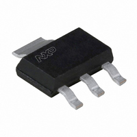
BSP33,115 NXP Semiconductors, BSP33,115 Datasheet - Page 3

BSP33,115
Manufacturer Part Number
BSP33,115
Description
TRANS PNP 80V 1000MA SOT223
Manufacturer
NXP Semiconductors
Series
-r
Datasheet
1.BSP31115.pdf
(6 pages)
Specifications of BSP33,115
Package / Case
SOT-223 (3 leads + Tab), SC-73, TO-261
Transistor Type
PNP
Current - Collector (ic) (max)
1A
Voltage - Collector Emitter Breakdown (max)
80V
Vce Saturation (max) @ Ib, Ic
500mV @ 50mA, 500mA
Dc Current Gain (hfe) (min) @ Ic, Vce
100 @ 100mA, 5V
Power - Max
1.3W
Frequency - Transition
100MHz
Mounting Type
Surface Mount
Minimum Operating Temperature
- 65 C
Configuration
Single Dual Collector
Transistor Polarity
PNP
Mounting Style
SMD/SMT
Collector- Emitter Voltage Vceo Max
80 V
Emitter- Base Voltage Vebo
5 V
Maximum Dc Collector Current
1 A
Power Dissipation
1300 mW
Maximum Operating Frequency
100 MHz
Maximum Operating Temperature
+ 150 C
Current - Collector Cutoff (max)
-
Lead Free Status / RoHS Status
Lead free / RoHS Compliant
Current - Collector Cutoff (max)
-
Lead Free Status / Rohs Status
Lead free / RoHS Compliant
Other names
933981990115
BSP33 T/R
BSP33 T/R
BSP33 T/R
BSP33 T/R
NXP Semiconductors
THERMAL CHARACTERISTICS
Note
1. Device mounted on a printed-circuit board, single sided copper, tinplated, mounting pad for collector 1 cm
CHARACTERISTICS
T
Note
1. Pulse test: t
1999 Apr 26
R
R
I
I
h
V
V
C
C
f
Switching times (between 10% and 90% levels)
t
t
SYMBOL
SYMBOL
amb
CBO
EBO
T
on
off
FE
CEsat
BEsat
PNP medium power transistors
th j-a
th j-s
c
e
For other mounting conditions, see “Thermal considerations for SOT223 in the General Part of associated
Handbook”.
= 25 °C unless otherwise specified.
thermal resistance from junction to ambient
thermal resistance from junction to soldering point
collector cut-off current
emitter cut-off current
DC current gain
DC current gain
collector-emitter saturation voltage I
base-emitter saturation voltage
collector capacitance
emitter capacitance
transition frequency
turn-on time
turn-off time
BSP32
BSP31; BSP33
p
≤ 300 μs; δ ≤ 0.01.
PARAMETER
PARAMETER
I
I
I
I
I
I
I
I
I
I
IC = −150 mA; IB = −15 mA; note 1
I
I
I
I
I
E
E
C
C
C
C
C
C
C
C
C
C
E
C
C
Con
= 0; V
= 0; V
= i
= 0; V
= −100 μA; V
= −100 mA; V
= −500 mA; V
= −100 μA; V
= −100 mA; V
= −500 mA; V
= −150 mA; I
= −500 mA; I
= −500 mA; I
= i
= −50 mA; V
= −100 mA; I
e
c
= 0; V
= 0; V
CB
CB
EB
3
= −60 V
= −60 V; T
= −5 V
CB
EB
CONDITIONS
CE
note 1
= −0.5 V; f = 1 MHz
B
B
B
= −10 V; f = 1 MHz
CE
CE
CE
CE
CE
CE
= −15 mA; note 1
= −50 mA; note 1
= −50 mA; note 1
Bon
= −10 V; f = 100 MHz
CONDITIONS
= −5 V; note 1
= −5 V; note 1
= −5 V; note 1
= −5 V; note 1
= −5 V; note 1
= −5 V; note 1
= −5 mA; I
j
= 150 °C
Boff
BSP31; BSP32; BSP33
= 5 mA
VALUE
93
12
−
−
−
10
40
30
30
100
50
−
−
−
−
−
−
100
−
−
MIN.
Product data sheet
−100
−50
−100
−
120
−
−
300
−
−250
−500
−1
−1.2
20
120
−
500
650
MAX.
UNIT
K/W
K/W
2
.
nA
μA
nA
mV
mV
V
V
pF
pF
MHz
ns
ns
UNIT


