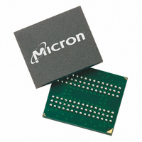
MT48LC4M32B2B5-7 IT:G Micron Technology Inc, MT48LC4M32B2B5-7 IT:G Datasheet - Page 51

MT48LC4M32B2B5-7 IT:G
Manufacturer Part Number
MT48LC4M32B2B5-7 IT:G
Description
DRAM Chip SDRAM 128M-Bit 4Mx32 3.3V 90-Pin VFBGA Tray
Manufacturer
Micron Technology Inc
Type
SDRAMr
Datasheet
1.MT48LC4M32B2P-7G_TR.pdf
(67 pages)
Specifications of MT48LC4M32B2B5-7 IT:G
Density
128 Mb
Maximum Clock Rate
143 MHz
Package
90VFBGA
Address Bus Width
14 Bit
Operating Supply Voltage
3.3 V
Maximum Random Access Time
17|8|5.5 ns
Operating Temperature
-40 to 85 °C
Format - Memory
RAM
Memory Type
SDRAM
Memory Size
128M (4Mx32)
Speed
143MHz
Interface
Parallel
Voltage - Supply
3 V ~ 3.6 V
Package / Case
90-VFBGA
Organization
4Mx32
Address Bus
14b
Access Time (max)
17/8/5.5ns
Operating Supply Voltage (typ)
3.3V
Package Type
VFBGA
Operating Temp Range
-40C to 85C
Operating Supply Voltage (max)
3.6V
Operating Supply Voltage (min)
3V
Supply Current
175mA
Pin Count
90
Mounting
Surface Mount
Operating Temperature Classification
Industrial
Lead Free Status / RoHS Status
Lead free / RoHS Compliant
Figure 34:
PDF: 09005aef80872800/Source: 09005aef80863355
128MbSDRAMx32_2.fm - Rev. L 1/09 EN
COMMAND
A0-A9, A11
Precharge all
BA0, BA1
DQM 0-3
active banks
CLK
CKE
A10
DQ
Power-Down Mode
t CMS
High-Z
t CKS
t AS
SINGLE BANK
PRECHARGE
ALL BANKS
BANK(S)
Notes:
T0
t CMH
t CKH
t AH
Two clock cycles
1. Violating refresh requirements during power-down may result in a loss of data.
All banks idle, enter
power-down mode
t CK
T1
NOP
t CKS
t CL
T2
NOP
Input buffers gated off while in
power-down mode
t CH
51
Exit power-down mode
(
(
(
(
(
(
)
)
)
(
)
(
)
(
(
(
)
(
)
)
)
)
)
)
(
(
(
(
(
(
(
(
)
)
(
)
(
)
(
)
(
)
(
)
)
(
)
)
)
)
)
Micron Technology, Inc., reserves the right to change products or specifications without notice.
(
(
)
)
)
t CKS
Tn + 1
NOP
All banks idle
©2001 Micron Technology, Inc. All rights reserved.
128Mb: x32 SDRAM
Timing Diagrams
Tn + 2
ACTIVE
ROW
ROW
BANK
DON’T CARE
UNDEFINED


