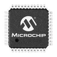
PIC16LF1517-E/PT Microchip Technology, PIC16LF1517-E/PT Datasheet - Page 100

PIC16LF1517-E/PT
Manufacturer Part Number
PIC16LF1517-E/PT
Description
40-pin, 14KB Flash, 512B RAM, 10-bit ADC, 2xCCP, SPI, MI2C, EUSART, 1.8V-3.6V 44
Manufacturer
Microchip Technology
Series
PIC® XLP™ 16Fr
Datasheet
1.PIC16LF1517-IPT.pdf
(344 pages)
Specifications of PIC16LF1517-E/PT
Core Processor
PIC
Core Size
8-Bit
Speed
20MHz
Connectivity
I²C, LIN, SPI, UART/USART
Peripherals
Brown-out Detect/Reset, POR, PWM, WDT
Number Of I /o
36
Program Memory Size
14KB (8K x 14)
Program Memory Type
FLASH
Ram Size
512 x 8
Voltage - Supply (vcc/vdd)
1.8 V ~ 3.6 V
Data Converters
A/D 28x10b
Oscillator Type
Internal
Operating Temperature
-40°C ~ 125°C
Package / Case
*
Processor Series
PIC16LF151x
Core
PIC
Data Bus Width
8 bit
Data Ram Size
512 B
Interface Type
I2C, SPI, USART
Maximum Clock Frequency
20 MHz
Number Of Programmable I/os
36
Number Of Timers
3
Operating Supply Voltage
1.8 V to 3.6 V
Maximum Operating Temperature
+ 125 C
Mounting Style
SMD/SMT
Lead Free Status / RoHS Status
Lead free / RoHS Compliant
Eeprom Size
-
Lead Free Status / Rohs Status
Details
Available stocks
Company
Part Number
Manufacturer
Quantity
Price
Company:
Part Number:
PIC16LF1517-E/PT
Manufacturer:
Microchip Technology
Quantity:
10 000
- Current page: 100 of 344
- Download datasheet (3Mb)
PIC16(L)F1516/7/8/9
11.2.2
The unlock sequence is a mechanism that protects the
Flash program memory from unintended self-write pro-
gramming or erasing. The sequence must be executed
and completed without interruption to successfully
complete any of the following operations:
• Row Erase
• Load program memory write latches
• Write of program memory write latches to pro-
• Write of program memory write latches to User
The unlock sequence consists of the following steps:
1. Write 55h to PMCON2
2. Write AAh to PMCON2
3. Set the WR bit in PMCON1
4. NOP instruction
5. NOP instruction
Once the WR bit is set, the processor will always force
two NOP instructions. When an Erase Row or Program
Row operation is being performed, the processor will stall
internal operations (typical 2 ms), until the operation is
complete and then resume with the next instruction.
When the operation is loading the program memory write
latches, the processor will always force the two NOP
instructions and continue uninterrupted with the next
instruction.
Since the unlock sequence must not be interrupted,
global interrupts should be disabled prior to the unlock
sequence and re-enabled after the unlock sequence is
completed.
DS41452A-page 100
gram memory
IDs
FLASH MEMORY UNLOCK
SEQUENCE
Preliminary
FIGURE 11-3:
WRITE or ERASE operation
Instruction Fetched ignored
Instruction Fetched ignored
NOP execution forced
NOP execution forced
Unlock Sequence
Unlock Sequence
Write 0AAh to
Write 055h to
FLASH PROGRAM
MEMORY UNLOCK
SEQUENCE FLOWCHART
PMCON2
PMCON2
(WR = 1)
2010 Microchip Technology Inc.
Initiate
Start
End
Related parts for PIC16LF1517-E/PT
Image
Part Number
Description
Manufacturer
Datasheet
Request
R

Part Number:
Description:
IC, 8BIT MCU, PIC16LF, 32MHZ, QFN-28
Manufacturer:
Microchip Technology
Datasheet:

Part Number:
Description:
IC, 8BIT MCU, PIC16LF, 32MHZ, QFN-28
Manufacturer:
Microchip Technology
Datasheet:

Part Number:
Description:
IC, 8BIT MCU, PIC16LF, 32MHZ, DIP-18
Manufacturer:
Microchip Technology
Datasheet:

Part Number:
Description:
IC, 8BIT MCU, PIC16LF, 20MHZ, TQFP-44
Manufacturer:
Microchip Technology
Datasheet:

Part Number:
Description:
7 KB Flash, 384 Bytes RAM, 32 MHz Int. Osc, 16 I/0, Enhanced Mid Range Core, Nan
Manufacturer:
Microchip Technology

Part Number:
Description:
14KB Flash, 512B RAM, LCD, 11x10b ADC, EUSART, NanoWatt XLP 28 SOIC .300in T/R
Manufacturer:
Microchip Technology
Datasheet:

Part Number:
Description:
14KB Flash, 512B RAM, LCD, 11x10b ADC, EUSART, NanoWatt XLP 28 SSOP .209in T/R
Manufacturer:
Microchip Technology
Datasheet:

Part Number:
Description:
MCU PIC 14KB FLASH XLP 28-SSOP
Manufacturer:
Microchip Technology

Part Number:
Description:
MCU PIC 14KB FLASH XLP 28-SOIC
Manufacturer:
Microchip Technology

Part Number:
Description:
MCU PIC 512B FLASH XLP 28-UQFN
Manufacturer:
Microchip Technology

Part Number:
Description:
MCU PIC 14KB FLASH XLP 28-SPDIP
Manufacturer:
Microchip Technology

Part Number:
Description:
MCU 7KB FLASH 256B RAM 40-UQFN
Manufacturer:
Microchip Technology

Part Number:
Description:
MCU 7KB FLASH 256B RAM 44-TQFP
Manufacturer:
Microchip Technology

Part Number:
Description:
MCU 14KB FLASH 1KB RAM 28-UQFN
Manufacturer:
Microchip Technology

Part Number:
Description:
MCU PIC 14KB FLASH XLP 40-UQFN
Manufacturer:
Microchip Technology


