PIC18LF13K22-E/SS Microchip Technology, PIC18LF13K22-E/SS Datasheet - Page 107
PIC18LF13K22-E/SS
Manufacturer Part Number
PIC18LF13K22-E/SS
Description
8KB Flash, 256bytes RAM, 256bytes EEPROM, 16MIPS, NanoWatt XLP 20 SSOP .209in TU
Manufacturer
Microchip Technology
Series
PIC® XLP™ 18Fr
Datasheets
1.PIC18LF13K22-ISS.pdf
(388 pages)
2.PIC18LF13K22-ISS.pdf
(12 pages)
3.PIC18LF13K22-ISS.pdf
(36 pages)
Specifications of PIC18LF13K22-E/SS
Core Processor
PIC
Core Size
8-Bit
Speed
48MHz
Connectivity
I²C, LIN, SPI, UART/USART
Peripherals
Brown-out Detect/Reset, POR, PWM, WDT
Number Of I /o
17
Program Memory Size
8KB (4K x 16)
Program Memory Type
FLASH
Eeprom Size
256 x 8
Ram Size
256 x 8
Voltage - Supply (vcc/vdd)
1.8 V ~ 3.6 V
Data Converters
A/D 12x10b
Oscillator Type
Internal
Operating Temperature
-40°C ~ 125°C
Package / Case
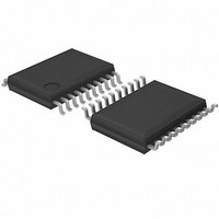
20-SSOP
Processor Series
PIC18LF
Core
PIC
Data Bus Width
8 bit
Data Ram Size
256 B
Interface Type
EUSART, I2C, SPI
Maximum Clock Frequency
32 KHz
Number Of Programmable I/os
18
Number Of Timers
4
Operating Supply Voltage
1.8 V to 3.6 V
Maximum Operating Temperature
+ 125 C
Mounting Style
SMD/SMT
3rd Party Development Tools
52715-96, 52716-328, 52717-734, 52712-325, EWPIC18
Development Tools By Supplier
PG164130, DV164035, DV244005, DV164005
Minimum Operating Temperature
- 40 C
On-chip Adc
10 bit, 12 Channel
Lead Free Status / RoHS Status
Lead free / RoHS Compliant
Lead Free Status / RoHS Status
Lead free / RoHS Compliant


11.0
The Timer2 module timer incorporates the following
features:
• 8-bit timer and period registers (TMR2 and PR2,
• Readable and writable (both registers)
• Software programmable prescaler (1:1, 1:4 and
• Software programmable postscaler (1:1 through
• Interrupt on TMR2-to-PR2 match
• Optional use as the shift clock for the MSSP
The module is controlled through the T2CON register
(Register 11-1), which enables or disables the timer
and configures the prescaler and postscaler. Timer2
can be shut off by clearing control bit, TMR2ON of the
T2CON register, to minimize power consumption.
A simplified block diagram of the module is shown in
Figure 11-1.
REGISTER 11-1:
2010 Microchip Technology Inc.
bit 7
Legend:
R = Readable bit
-n = Value at POR
bit 7
bit 6-3
bit 2
bit 1-0
respectively)
1:16)
1:16)
module
U-0
—
TIMER2 MODULE
Unimplemented: Read as ‘0’
T2OUTPS<3:0>: Timer2 Output Postscale Select bits
0000 = 1:1 Postscale
0001 = 1:2 Postscale
•
•
•
1111 = 1:16 Postscale
TMR2ON: Timer2 On bit
1 = Timer2 is on
0 = Timer2 is off
T2CKPS<1:0>: Timer2 Clock Prescale Select bits
00 = Prescaler is 1
01 = Prescaler is 4
1x = Prescaler is 16
T2OUTPS3
R/W-0
T2CON: TIMER2 CONTROL REGISTER
W = Writable bit
‘1’ = Bit is set
T2OUTPS2
R/W-0
T2OUTPS1
R/W-0
Preliminary
PIC18F1XK22/LF1XK22
U = Unimplemented bit, read as ‘0’
‘0’ = Bit is cleared
T2OUTPS0
R/W-0
11.1
In normal operation, TMR2 is incremented from 00h on
each clock (F
clock input gives direct input, divide-by-4 and
divide-by-16 prescale options; these are selected by
the prescaler control bits, T2CKPS<1:0> of the T2CON
register. The value of TMR2 is compared to that of the
period register, PR2, on each clock cycle. When the
two values match, the comparator generates a match
signal as the timer output. This signal also resets the
value of TMR2 to 00h on the next cycle and drives the
output counter/postscaler (see Section 11.2 “Timer2
Interrupt”).
The TMR2 and PR2 registers are both directly readable
and writable. The TMR2 register is cleared on any
device Reset, whereas the PR2 register initializes to
FFh. Both the prescaler and postscaler counters are
cleared on the following events:
• a write to the TMR2 register
• a write to the T2CON register
• any device Reset (Power-on Reset, MCLR Reset,
TMR2 is not cleared when T2CON is written.
Watchdog Timer Reset or Brown-out Reset)
Timer2 Operation
TMR2ON
OSC
R/W-0
/4). A 4-bit counter/prescaler on the
x = Bit is unknown
T2CKPS1
R/W-0
DS41365D-page 107
T2CKPS0
R/W-0
bit 0
Related parts for PIC18LF13K22-E/SS
Image
Part Number
Description
Manufacturer
Datasheet
Request
R

Part Number:
Description:
Manufacturer:
Microchip Technology Inc.
Datasheet:
Part Number:
Description:
Manufacturer:
Microchip Technology Inc.
Datasheet:
Part Number:
Description:
Manufacturer:
Microchip Technology Inc.
Datasheet:
Part Number:
Description:
Manufacturer:
Microchip Technology Inc.
Datasheet:
Part Number:
Description:
Manufacturer:
Microchip Technology Inc.
Datasheet:
Part Number:
Description:
Manufacturer:
Microchip Technology Inc.
Datasheet:
Part Number:
Description:
Manufacturer:
Microchip Technology Inc.
Datasheet:
Part Number:
Description:
Manufacturer:
Microchip Technology Inc.
Datasheet: