PIC18LF13K22-E/SS Microchip Technology, PIC18LF13K22-E/SS Datasheet - Page 58
PIC18LF13K22-E/SS
Manufacturer Part Number
PIC18LF13K22-E/SS
Description
8KB Flash, 256bytes RAM, 256bytes EEPROM, 16MIPS, NanoWatt XLP 20 SSOP .209in TU
Manufacturer
Microchip Technology
Series
PIC® XLP™ 18Fr
Datasheets
1.PIC18LF13K22-ISS.pdf
(388 pages)
2.PIC18LF13K22-ISS.pdf
(12 pages)
3.PIC18LF13K22-ISS.pdf
(36 pages)
Specifications of PIC18LF13K22-E/SS
Core Processor
PIC
Core Size
8-Bit
Speed
48MHz
Connectivity
I²C, LIN, SPI, UART/USART
Peripherals
Brown-out Detect/Reset, POR, PWM, WDT
Number Of I /o
17
Program Memory Size
8KB (4K x 16)
Program Memory Type
FLASH
Eeprom Size
256 x 8
Ram Size
256 x 8
Voltage - Supply (vcc/vdd)
1.8 V ~ 3.6 V
Data Converters
A/D 12x10b
Oscillator Type
Internal
Operating Temperature
-40°C ~ 125°C
Package / Case
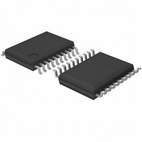
20-SSOP
Processor Series
PIC18LF
Core
PIC
Data Bus Width
8 bit
Data Ram Size
256 B
Interface Type
EUSART, I2C, SPI
Maximum Clock Frequency
32 KHz
Number Of Programmable I/os
18
Number Of Timers
4
Operating Supply Voltage
1.8 V to 3.6 V
Maximum Operating Temperature
+ 125 C
Mounting Style
SMD/SMT
3rd Party Development Tools
52715-96, 52716-328, 52717-734, 52712-325, EWPIC18
Development Tools By Supplier
PG164130, DV164035, DV244005, DV164005
Minimum Operating Temperature
- 40 C
On-chip Adc
10 bit, 12 Channel
Lead Free Status / RoHS Status
Lead free / RoHS Compliant
Lead Free Status / RoHS Status
Lead free / RoHS Compliant


PIC18F1XK22/LF1XK22
EXAMPLE 4-3:
4.5.2
Depending on the application, good programming
practice may dictate that the value written to the
memory should be verified against the original value.
This should be used in applications where excessive
writes can stress bits near the specification limit.
4.5.3
If a write is terminated by an unplanned event, such as
loss of power or an unexpected Reset, the memory
location just programmed should be verified and
reprogrammed if needed. If the write operation is
interrupted by a MCLR Reset or a WDT Time-out Reset
during normal operation, the WRERR bit will be set
which the user can check to decide whether a rewrite
of the location(s) is needed.
TABLE 4-3:
DS41365D-page 58
EECON1
EECON2
INTCON
IPR2
PIE2
PIR2
TABLAT
TBLPTRL Program Memory Table Pointer Low Byte (TBLPTR<7:0>)
TBLPTRU
TBPLTRH Program Memory Table Pointer High Byte (TBLPTR<15:8>)
Legend: — = unimplemented, read as ‘0’. Shaded cells are not used during Flash/EEPROM access.
PROGRAM_MEMORY
Name
Required
Sequence
WRITE VERIFY
UNEXPECTED TERMINATION OF
WRITE OPERATION
EEPROM Control Register 2 (not a physical register)
Program Memory Table Latch
GIE/GIEH PEIE/GIEL TMR0IE
OSCFIP
OSCFIE
OSCFIF
EEPGD
Bit 7
—
REGISTERS ASSOCIATED WITH PROGRAM FLASH MEMORY
DECFSZ
BRA
BSF
BCF
BSF
BCF
MOVLW
MOVWF
MOVLW
MOVWF
BSF
DCFSZ
BRA
BSF
BCF
WRITING TO FLASH PROGRAM MEMORY (CONTINUED)
CFGS
C1IP
C1IE
Bit 6
C1IF
—
COUNTER
WRITE_WORD_TO_HREGS
EECON1, EEPGD
EECON1, CFGS
EECON1, WREN
INTCON, GIE
55h
EECON2
0AAh
EECON2
EECON1, WR
COUNTER2
WRITE_BYTE_TO_HREGS
INTCON, GIE
EECON1, WREN
bit 21
C2IP
C2IE
Bit 5
C2IF
—
Program Memory Table Pointer Upper Byte (TBLPTR<20:16>)
INT0IE
FREE
EEIP
EEIE
Bit 4
EEIF
Preliminary
; loop until holding registers are full
; point to Flash program memory
; access Flash program memory
; enable write to memory
; disable interrupts
; write 55h
; write 0AAh
; start program (CPU stall)
; repeat for remaining write blocks
;
; re-enable interrupts
; disable write to memory
WRERR
RABIE
BCLIP
BCLIE
BCLIF
Bit 3
4.5.4
To protect against spurious writes to Flash program
memory, the write initiate sequence must also be
followed. See Section 22.0 “Special Features of the
CPU” for more detail.
4.6
See Section 22.3 “Program Verification and Code
Protection” for details on code protection of Flash
program memory.
TMR0IF
Flash Program Operation During
Code Protection
WREN
Bit 2
—
—
—
PROTECTION AGAINST
SPURIOUS WRITES
TMR3IP
TMR3IE
TMR3IF
INT0IF
Bit 1
WR
2010 Microchip Technology Inc.
RABIF
Bit 0
RD
—
—
—
Values on
Reset
page
259
259
257
260
260
260
257
257
257
257
Related parts for PIC18LF13K22-E/SS
Image
Part Number
Description
Manufacturer
Datasheet
Request
R

Part Number:
Description:
Manufacturer:
Microchip Technology Inc.
Datasheet:
Part Number:
Description:
Manufacturer:
Microchip Technology Inc.
Datasheet:
Part Number:
Description:
Manufacturer:
Microchip Technology Inc.
Datasheet:
Part Number:
Description:
Manufacturer:
Microchip Technology Inc.
Datasheet:
Part Number:
Description:
Manufacturer:
Microchip Technology Inc.
Datasheet:
Part Number:
Description:
Manufacturer:
Microchip Technology Inc.
Datasheet:
Part Number:
Description:
Manufacturer:
Microchip Technology Inc.
Datasheet:
Part Number:
Description:
Manufacturer:
Microchip Technology Inc.
Datasheet: