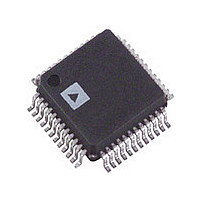
ADV7172KST Analog Devices Inc, ADV7172KST Datasheet - Page 6

ADV7172KST
Manufacturer Part Number
ADV7172KST
Description
Manufacturer
Analog Devices Inc
Datasheet
1.ADV7172KST.pdf
(60 pages)
Specifications of ADV7172KST
Number Of Dac's
6
Adc/dac Resolution
10b
Screening Level
Commercial
Package Type
LQFP
Pin Count
48
Lead Free Status / RoHS Status
Not Compliant
Available stocks
Company
Part Number
Manufacturer
Quantity
Price
Company:
Part Number:
ADV7172KST
Manufacturer:
SUN
Quantity:
5 000
Company:
Part Number:
ADV7172KST
Manufacturer:
ADI
Quantity:
850
Part Number:
ADV7172KST
Manufacturer:
ADI/亚德诺
Quantity:
20 000
Company:
Part Number:
ADV7172KSTZ
Manufacturer:
AD
Quantity:
80
Part Number:
ADV7172KSTZ
Manufacturer:
ADI/亚德诺
Quantity:
20 000
Company:
Part Number:
ADV7172KSTZ-REEL
Manufacturer:
Analog Devices Inc
Quantity:
10 000
ADV7172/ADV7173
5 V TIMING SPECIFICATIONS
Parameter
MPU PORT
ANALOG OUTPUTS
CLOCK CONTROL AND
PIXEL PORT
TELETEXT PORT
RESET CONTROL
NOTES
1
2
3
4
5
6
7
Specifications subject to change without notice.
The max/min specifications are guaranteed over this range. The max/min values are typical over 4.75 V to 5.25 V.
Temperature range T
TTL input values are 0 to 3 volts, with input rise/fall times ≤ 3 ns, measured between the 10% and 90% points. Timing reference points at 50% for inputs and
Guaranteed by characterization.
Output delay measured from the 50% point of the rising edge of CLOCK to the 50% point of full-scale transition.
Pixel Port consists of the following:
Teletext Port consists of the following:
outputs. Analog output load ≤ 10 pF.
Pixel Inputs:
Pixel Controls:
Clock Input:
Teletext Output:
Teletext Input:
SCLOCK Frequency
SCLOCK High Pulsewidth, t
SCLOCK Low Pulsewidth, t
Hold Time (Start Condition), t
Setup Time (Start Condition), t
Data Setup Time, t
SDATA, SCLOCK Rise Time, t
SDATA, SCLOCK Fall Time, t
Setup Time (Stop Condition), t
Analog Output Delay
DAC Analog Output Skew
f
Clock High Time, t
Clock Low Time, t
Data Setup Time, t
Data Hold Time, t
Control Setup Time, t
Control Hold Time, t
Digital Output Access Time, t
Digital Output Hold Time, t
Pipeline Delay, t
Digital Output Access Time, t
Data Setup Time, t
Data Hold Time, t
RESET Low Time
CLOCK
3, 4
5, 6
MIN
15
P7–P0
HSYNC, FIELD/VSYNC, BLANK, VSO, CSO_HSO, CLAMP
CLOCK
TTXREQ
TTX
3, 7
3
12
18
to T
10
5
11
17
9
3, 5
12
11
MAX
: 0°C to 70°C.
14
2
1
13
16
3
8
4
7
6
Conditions
After this period the 1st clock is generated
relevant for repeated Start Condition.
(V
to T
AA
MAX
= 5 V
2
unless otherwise noted.)
5%
1
, V
REF
= 1.235 V, R
SET1
= 600
unless otherwise noted. All specifications T
Min
0
0.6
1.3
0.6
0.6
100
0.6
8
8
4.0
5.0
4
3
Typ
7
0
27
15
10
37
20
2
6
3
Max
400
300
300
24
Unit
µs
µs
µs
µs
ns
ns
ns
µs
ns
ns
MHz
ns
ns
ns
ns
ns
ns
ns
ns
Clock Cycles
ns
ns
ns
ns
kHz
MIN


