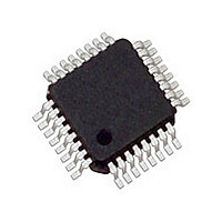
MC33910G5AC Freescale, MC33910G5AC Datasheet - Page 80

MC33910G5AC
Manufacturer Part Number
MC33910G5AC
Description
Manufacturer
Freescale
Datasheet
1.MC33910G5AC.pdf
(90 pages)
Specifications of MC33910G5AC
Turn Off Delay Time
10us
Number Of Drivers
2
Operating Temperature (min)
-40C
Operating Temperature (max)
125C
Operating Temperature Classification
Automotive
Lead Free Status / RoHS Status
Compliant
Available stocks
Company
Part Number
Manufacturer
Quantity
Price
Company:
Part Number:
MC33910G5AC
Manufacturer:
Freescale Semiconductor
Quantity:
10 000
Part Number:
MC33910G5AC
Manufacturer:
FREESCALE
Quantity:
20 000
Company:
Part Number:
MC33910G5ACR2
Manufacturer:
Freescale Semiconductor
Quantity:
10 000
MOD2, MOD1 - Mode Control Bits
to clear the watchdog in accordance with
Control Bits.
Table 40.
Voltage Status Register - VSR
register is also returned when writing to the MCR.
VSOV - V
the VS1 pin.
VSUV - V
the VS1 pin.
VDDOT - Main Voltage Regulator Over-temperature
Warning
temperature reached the Over-Temperature Prewarning
Threshold.
BATFAIL - Battery Fail Flag.
the 33910 had a power on reset (POR).
Analog Integrated Circuit Device Data
Freescale Semiconductor
MOD2
These write-only bits select the Operating mode and allow
Returns the status of the several voltage monitors. This
This read-only bit indicates an over-voltage condition on
1 = Over-voltage condition.
0 = Normal condition.
This read-only bit indicates an under-voltage condition on
1 = Under-voltage condition.
0 = Normal condition.
This read-only bit indicates that the main voltage regulator
1 = Over-temperature prewarning
0 = Normal
This read-only bit is set during power-up and indicates that
0
0
1
1
Table 41. Voltage Status Register - $0/$1
SUP
SUP
Read
Mode Control Bits
MOD1
Under-voltage
Over-voltage
0
1
0
1
VSOV
S3
Normal Mode + watchdog Clear
VSUV
S2
Normal Mode
Description
Sleep Mode
Stop Mode
VDDOT
S1
Table 38
BATFAIL
S0
Mode
will clear the BATFAIL flag.
Wake-up Control Register - WUCR
Writing the wake-up control register (WUCR) will return the
wake-up status register (WUSR).
Table 42.
L1WE - Wake-up Input Enable
and Sleep mode the L1WE bit activates the L1 input for wake-
up. If the L1 input is selected on the analog multiplexer, the
L1WE is masked to 0.
Wake-up Status Register - WUSR
and is also returned when writing to the wake-up control
register (WUCR).
L1 - Wake-up input
L1 input is not enabled then the wake-up status will return 0.
allows to verify the L1 input has caused the wake-up, by first
reading the interrupt status register (ISR) and then reading
the wake-up status register (WUSR).
Any access to the MCR or voltage status register (VSR)
1 = POR Reset has occurred
0 = POR Reset has not occurred
This register is used to control the digital wake-up input.
This write-only bit enables/disables the L1 input. In Stop
1 = Wake-up Input enabled.
0 = Wake-up Input disabled.
This register is used to monitor the digital wake-up inputs
This read-only bit indicates the status of the L1 input. If the
After a wake-up form Stop or Sleep mode this bit also
1 = L1 Wake-up.
0 = L1 Wake-up disabled or selected as analog input.
Table 43. Wake-up Status Register - $2/$3
Condition
Reset
Value
Reset
Write
Read
Wake-up Control Register - $2
C3
S3
0
1
-
POR, Reset mode or ext_reset
LOGIC COMMANDS AND REGISTERS
FUNCTIONAL DEVICE OPERATIONS
C2
S2
0
1
-
C1
S1
0
1
-
L1WE
C0
S0
L1
1
33910
80


