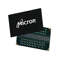
MT47H32M16HR-3 IT:F Micron Technology Inc, MT47H32M16HR-3 IT:F Datasheet - Page 17

MT47H32M16HR-3 IT:F
Manufacturer Part Number
MT47H32M16HR-3 IT:F
Description
MICMT47H32M16HR-3_IT:F 32MBX16 DDR2
Manufacturer
Micron Technology Inc
Type
DDR2 SDRAMr
Datasheet
1.MT47H32M16HR-3_ITF.pdf
(132 pages)
Specifications of MT47H32M16HR-3 IT:F
Organization
32Mx16
Density
512Mb
Address Bus
15b
Access Time (max)
450ps
Maximum Clock Rate
667MHz
Operating Supply Voltage (typ)
1.8V
Package Type
FBGA
Operating Temp Range
-40C to 85C
Operating Supply Voltage (max)
1.9V
Operating Supply Voltage (min)
1.7V
Supply Current
250mA
Pin Count
84
Mounting
Surface Mount
Operating Temperature Classification
Industrial
Lead Free Status / RoHS Status
Compliant
- Current page: 17 of 132
- Download datasheet (10Mb)
Table 3: FBGA 84-Ball – x16 and 60-Ball – x4, x8 Descriptions (Continued)
PDF: 09005aef82f1e6e2
512MbDDR2.pdf - Rev. R 12/10 EN
UDQS, UDQS#
RDQS, RDQS#
LDQS, LDQS#
DQS, DQS#
Symbol
V
V
V
V
V
RFU
V
V
NC
NU
NF
DDQ
SSDL
DDL
REF
SSQ
DD
SS
Output
Supply
Supply
Supply
Supply
Supply
Supply
Supply
Type
I/O
I/O
I/O
–
–
–
–
Description
Data strobe: Output with read data, input with write data for source synchronous oper-
ation. Edge-aligned with read data, center-aligned with write data. DQS# is only used
when differential data strobe mode is enabled via the LOAD MODE command.
Data strobe for lower byte: Output with read data, input with write data for source
synchronous operation. Edge-aligned with read data, center-aligned with write data.
LDQS# is only used when differential data strobe mode is enabled via the LOAD MODE
command.
Data strobe for upper byte: Output with read data, input with write data for source
synchronous operation. Edge-aligned with read data, center-aligned with write data.
UDQS# is only used when differential data strobe mode is enabled via the LOAD MODE
command.
Redundant data strobe: For 64 Meg x 8 only. RDQS is enabled/disabled via the load
mode command to the extended mode register (EMR). When RDQS is enabled, RDQS is
output with read data only and is ignored during write data. When RDQS is disabled, ball
B3 becomes data mask (see DM ball). RDQS# is only used when RDQS is enabled and dif-
ferential data strobe mode is enabled.
Power supply: 1.8V ±0.1V.
DQ power supply: 1.8V ±0.1V. Isolated on the device for improved noise immunity.
DLL power supply: 1.8V ±0.1V.
SSTL_18 reference voltage (V
Ground.
DLL ground: Isolated on the device from V
DQ ground: Isolated on the device for improved noise immunity.
No connect: These balls should be left unconnected.
No function: x8: these balls are used as DQ[7:4]; x4: they are no function.
Not used: If EMR(E10) = 0: x16, A8 = UDQS# and E8 = LDQS#; x8, A2 = RDQS# and A8 =
DQS#; x4, A2 = NU and A8 = NU. If EMR(E10) = 1: x16, A8 = NU and E8 = NU; x8, A2 = NU
and A8 = NU; x4, A2 = NU and A8 = NU.
Reserved for future use: Bank address BA2, row address bits A13 (x16 only), A14, and
A15.
17
DDQ
/2).
Micron Technology, Inc. reserves the right to change products or specifications without notice.
Ball Assignments and Descriptions
512Mb: x4, x8, x16 DDR2 SDRAM
SS
and V
SSQ
.
© 2004 Micron Technology, Inc. All rights reserved.
Related parts for MT47H32M16HR-3 IT:F
Image
Part Number
Description
Manufacturer
Datasheet
Request
R

Part Number:
Description:
IC SDRAM 64MBIT 133MHZ 54TSOP
Manufacturer:
Micron Technology Inc
Datasheet:

Part Number:
Description:
IC SDRAM 64MBIT 5.5NS 86TSOP
Manufacturer:
Micron Technology Inc
Datasheet:

Part Number:
Description:
IC SDRAM 64MBIT 200MHZ 86TSOP
Manufacturer:
Micron Technology Inc
Datasheet:

Part Number:
Description:
IC SDRAM 64MBIT 133MHZ 54TSOP
Manufacturer:
Micron Technology Inc
Datasheet:

Part Number:
Description:
IC SDRAM 128MBIT 133MHZ 54TSOP
Manufacturer:
Micron Technology Inc
Datasheet:

Part Number:
Description:
IC SDRAM 256MBIT 133MHZ 90VFBGA
Manufacturer:
Micron Technology Inc
Datasheet:

Part Number:
Description:
IC SDRAM 128MBIT 133MHZ 54TSOP
Manufacturer:
Micron Technology Inc
Datasheet:

Part Number:
Description:
IC SDRAM 256MBIT 133MHZ 54TSOP
Manufacturer:
Micron Technology Inc
Datasheet:

Part Number:
Description:
IC DDR SDRAM 512MBIT 6NS 66TSOP
Manufacturer:
Micron Technology Inc
Datasheet:

Part Number:
Description:
IC SDRAM 128MBIT 167MHZ 86TSOP
Manufacturer:
Micron Technology Inc
Datasheet:

Part Number:
Description:
IC SDRAM 128MBIT 143MHZ 86TSOP
Manufacturer:
Micron Technology Inc
Datasheet:

Part Number:
Description:
SDRAM 256M-BIT 1.8V 54-PIN VFBGA
Manufacturer:
Micron Technology Inc
Datasheet:

Part Number:
Description:
IC SDRAM 128MBIT 143MHZ 86TSOP
Manufacturer:
Micron Technology Inc
Datasheet:

Part Number:
Description:
IC SDRAM 128MBIT 125MHZ 54VFBGA
Manufacturer:
Micron Technology Inc
Datasheet:

Part Number:
Description:
IC SDRAM 128MBIT 125MHZ 54VFBGA
Manufacturer:
Micron Technology Inc
Datasheet:


