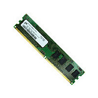
MT8HTF12864AY-667E1 Micron Technology Inc, MT8HTF12864AY-667E1 Datasheet

MT8HTF12864AY-667E1
Specifications of MT8HTF12864AY-667E1
Related parts for MT8HTF12864AY-667E1
MT8HTF12864AY-667E1 Summary of contents
Page 1
... DDR2 SDRAM UDIMM MT8HTF3264AY – 256MB MT8HTF6464AY – 512MB MT8HTF12864AY – 1GB Features • 240-pin, unbuffered dual in-line memory module • Fast data transfer rates: PC2-3200, PC2-4200, PC2-5300, PC2-6400, or PC2-8500 • 256MB (32 Meg x 64), 512MB (64 Meg x 64), or 1GB (128 Meg x 64 • ...
Page 2
... Table 2: Addressing Parameter Refresh count Row address Device bank address Device configuration 256Mb (32 Meg x 8) Column address Module rank address Table 3: Part Numbers and Timing Parameters – 256MB Modules (End of Life) 1 Base device: MT47H32M8, 256Mb DDR2 SDRAM Module 2 Part Number Density MT8HTF3264A(I)Y-667__ ...
Page 3
... The data sheet for the base device can be found on Micron’s Web site. Notes: 2. All part numbers end with a two-place code (not shown) that designates component and PCB revisions. Consult factory for current revision codes. Example: MT8HTF12864AY-667E1. PDF: 09005aef80e2ff8d htf8c32_64_128x64aypdf - Rev. G 3/10 EN ...
Page 4
Pin Assignments Table 6: Pin Assignments 240-Pin UDIMM Front Pin Symbol Pin Symbol Pin DQ19 61 REF DQ0 33 DQ24 63 4 DQ1 34 DQ25 ...
Page 5
... Pin Descriptions The pin description table below is a comprehensive list of all possible pins for all DDR2 modules. All pins listed may not be supported on this module. See Pin Assignments for information specific to this module. Table 7: Pin Descriptions Symbol Type Ax Input BAx Input ...
Page 6
... SPD EEPROM power supply: 1.7–3.6V. Reference voltage: V /2. DD Ground. No connect: These pins are not connected on the module. No function: These pins are connected within the module, but provide no functionality. Not used: These pins are not used in specific module configurations/operations. Reserved for future use. 6 Pin Descriptions and V ...
Page 7
Functional Block Diagram Figure 2: Functional Block Diagram – Raw Card D S0# DQS0 DQS0 DM0 DQ DQ0 DQ DQ1 DQ DQ2 DQ DQ3 DQ4 DQ DQ DQ5 DQ DQ6 DQ DQ7 DQS1# DQS1 DM1 DQ DQ8 DQ ...
Page 8
Figure 3: Functional Block Diagram – Alternate Clock S0# DQS0 DQS0 DM0 DQ DQ0 DQ DQ1 DQ DQ2 DQ DQ3 DQ4 DQ DQ DQ5 DQ DQ6 DQ DQ7 DQS1# DQS1 DM1 DQ DQ8 DQ DQ9 DQ DQ10 DQ ...
Page 9
... DRAM core and eight corresponding n-bit-wide, one-half-clock-cycle data trans- fers at the I/O pins. DDR2 modules use two sets of differential signals: DQS, DQS# to capture data and CK and CK# to capture commands, addresses, and control signals. Differential clocks and data strobes ensure exceptional noise immunity for these signals and provide precise crossing points to capture input signals ...
Page 10
... Electrical Specifications Stresses greater than those listed may cause permanent damage to the module. This is a stress rating only, and functional operation of the module at these or any other condi- tions outside those indicated in the device data sheet is not implied. Exposure to absolute maximum rating conditions for extended periods may adversely affect reliability. ...
Page 11
... Component specifications are available on Micron's Web site. Module speed grades cor- relate with component speed grades. Table 9: Module and Component Speed Grades DDR2 components may exceed the listed module speed grades; module may not be available in all listed speed grades Module Speed Grade -1GA ...
Page 12
I Specifications DD Table 10: DDR2 I Specifications and Conditions – 256MB DD Values shown for MT47H32M8 DDR2 SDRAM only and are computed from values specified in the 256Mb (32 Meg x 8) component data sheet Parameter Operating one bank ...
Page 13
Table 10: DDR2 I Specifications and Conditions – 256MB (Continued) DD Values shown for MT47H32M8 DDR2 SDRAM only and are computed from values specified in the 256Mb (32 Meg x 8) component data sheet Parameter Operating bank interleave read current: ...
Page 14
Table 11: DDR2 I Specifications and Conditions – 512MB DD Values shown for MT47H64M8 DDR2 SDRAM only and are computed from values specified in the 512Mb (64 Meg x 8) component data sheet Parameter Operating one bank active-precharge current: t ...
Page 15
Table 11: DDR2 I Specifications and Conditions – 512MB (Continued) DD Values shown for MT47H64M8 DDR2 SDRAM only and are computed from values specified in the 512Mb (64 Meg x 8) component data sheet Parameter Operating bank interleave read current: ...
Page 16
Table 12: DDR2 I Specifications and Conditions – 1GB DD Values shown for MT47H128M8 DDR2 SDRAM only and are computed from values specified in the 1Gb (128 Meg x 8) com- ponent data sheet Parameter Operating one bank active-precharge current: ...
Page 17
Serial Presence-Detect For the latest SPD data, refer to Micron's SPD page: www.micron.com/SPD. Table 13: SPD EEPROM Operating Conditions Parameter/Condition Supply voltage Input high voltage: logic 1; All inputs Input low voltage: logic 0; All inputs Output low voltage: I ...
Page 18
... FRONT VIEW 133.5 (5.256) 133.2 (5.244 0.76 (0.03) R 0.8 (0.031) TYP 123.0 (4.840) TYP BACK VIEW No Components This Side of Module 5.0 (0.197) TYP 63.0 (2.48) TYP additional design dimensions. times occur. 18 Module Dimensions U7 U8 30.5 (1.2) 29.85 (1.175) 17.78 (0.7) TYP 10 ...


