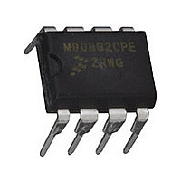
MC68HC908QT2CPE Freescale, MC68HC908QT2CPE Datasheet - Page 44

MC68HC908QT2CPE
Manufacturer Part Number
MC68HC908QT2CPE
Description
Manufacturer
Freescale
Datasheet
1.MC68HC908QT2CPE.pdf
(184 pages)
Specifications of MC68HC908QT2CPE
Cpu Family
HC08
Device Core Size
8b
Frequency (max)
8MHz
Total Internal Ram Size
128Byte
# I/os (max)
6
Number Of Timers - General Purpose
2
Operating Supply Voltage (typ)
3.3/5V
Operating Supply Voltage (max)
5.5V
Operating Supply Voltage (min)
2.7V
On-chip Adc
4-chx8-bit
Instruction Set Architecture
CISC
Operating Temp Range
-40C to 85C
Operating Temperature Classification
Industrial
Mounting
Through Hole
Pin Count
8
Package Type
PDIP
Program Memory Type
Flash
Program Memory Size
1.5KB
Lead Free Status / RoHS Status
Compliant
- Current page: 44 of 184
- Download datasheet (2Mb)
Analog-to-Digital Converter (ADC)
3.3.2 Voltage Conversion
When the input voltage to the ADC equals V
, the ADC converts the signal to $FF (full scale). If the input
DD
voltage equals V
the ADC converts it to $00. Input voltages between V
and V
are a straight-line
SS,
DD
SS
linear conversion. All other input voltages will result in $FF if greater than V
and $00 if less than V
.
DD
SS
NOTE
Input voltage should not exceed the analog supply voltages.
3.3.3 Conversion Time
Sixteen ADC internal clocks are required to perform one conversion. The ADC starts a conversion on the
first rising edge of the ADC internal clock immediately following a write to the ADSCR. If the ADC internal
clock is selected to run at 1 MHz, then one conversion will take 16 μs to complete. With a 1-MHz ADC
internal clock the maximum sample rate is 62.5 kHz.
16 ADC Clock Cycles
Conversion Time =
ADC Clock Frequency
Number of Bus Cycles = Conversion Time × Bus Frequency
3.3.4 Continuous Conversion
In the continuous conversion mode (ADCO = 1), the ADC continuously converts the selected channel
filling the ADC data register (ADR) with new data after each conversion. Data from the previous
conversion will be overwritten whether that data has been read or not. Conversions will continue until the
ADCO bit is cleared. The COCO bit (ADSCR, $003C) is set after each conversion and will stay set until
the next read of the ADC data register.
When a conversion is in process and the ADSCR is written, the current conversion data should be
discarded to prevent an incorrect reading.
3.3.5 Accuracy and Precision
The conversion process is monotonic and has no missing codes.
3.4 Interrupts
When the AIEN bit is set, the ADC module is capable of generating a central processor unit (CPU)
interrupt after each ADC conversion. A CPU interrupt is generated if the COCO bit is at 0. The COCO bit
is not used as a conversion complete flag when interrupts are enabled.
3.5 Low-Power Modes
The following subsections describe the ADC in low-power modes.
3.5.1 Wait Mode
The ADC continues normal operation during wait mode. Any enabled CPU interrupt request from the ADC
can bring the microcontroller unit (MCU) out of wait mode. If the ADC is not required to bring the MCU out
of wait mode, power down the ADC by setting the CH[4:0] bits in ADSCR to 1s before executing the WAIT
instruction.
MC68HC908QY/QT Family Data Sheet, Rev. 6
44
Freescale Semiconductor
Related parts for MC68HC908QT2CPE
Image
Part Number
Description
Manufacturer
Datasheet
Request
R

Part Number:
Description:
TOWER ELEVATOR BOARDS HARDWARE
Manufacturer:
Freescale Semiconductor
Datasheet:

Part Number:
Description:
TOWER SERIAL I/O HARDWARE
Manufacturer:
Freescale Semiconductor
Datasheet:

Part Number:
Description:
LCD MODULE FOR TWR SYSTEM
Manufacturer:
Freescale Semiconductor
Datasheet:

Part Number:
Description:
DAUGHTER LCD WVGA I.MX51
Manufacturer:
Freescale Semiconductor
Datasheet:

Part Number:
Description:
TOWER SYSTEM BOARD MPC5125
Manufacturer:
Freescale Semiconductor
Datasheet:

Part Number:
Description:
KIT EVALUATION I.MX51
Manufacturer:
Freescale Semiconductor
Datasheet:

Part Number:
Description:
KIT DEVELOPMENT WINCE IMX25
Manufacturer:
Freescale Semiconductor
Datasheet:

Part Number:
Description:
TOWER SYSTEM KIT MPC5125
Manufacturer:
Freescale Semiconductor
Datasheet:

Part Number:
Description:
TOWER SYSTEM BOARD K40X256
Manufacturer:
Freescale Semiconductor
Datasheet:

Part Number:
Description:
TOWER SYSTEM KIT K40X256
Manufacturer:
Freescale Semiconductor
Datasheet:

Part Number:
Description:
Microcontrollers (MCU) MX28 PLATFORM DEV KIT
Manufacturer:
Freescale Semiconductor
Datasheet:

Part Number:
Description:
MCU, MPU & DSP Development Tools IAR KickStart Kit for Kinetis K60
Manufacturer:
Freescale Semiconductor
Datasheet:

Part Number:
Description:
24BIT HDMI MX535/08
Manufacturer:
Freescale Semiconductor
Datasheet:
Part Number:
Description:
Manufacturer:
Freescale Semiconductor, Inc
Datasheet:
Part Number:
Description:
Manufacturer:
Freescale Semiconductor, Inc
Datasheet:


