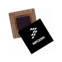
MPC8270CVVUPEA Freescale, MPC8270CVVUPEA Datasheet - Page 3

MPC8270CVVUPEA
Manufacturer Part Number
MPC8270CVVUPEA
Description
Manufacturer
Freescale
Datasheet
1.MPC8270CVVUPEA.pdf
(80 pages)
Specifications of MPC8270CVVUPEA
Family Name
MPC82XX
Device Core
PowerQUICC II
Device Core Size
32b
Frequency (max)
450MHz
Instruction Set Architecture
RISC
Operating Supply Voltage (max)
1.6V
Operating Supply Voltage (min)
1.45V
Operating Temp Range
-40C to 105C
Operating Temperature Classification
Industrial
Mounting
Surface Mount
Pin Count
480
Package Type
TBGA
Lead Free Status / RoHS Status
Compliant
Available stocks
Company
Part Number
Manufacturer
Quantity
Price
Company:
Part Number:
MPC8270CVVUPEA
Manufacturer:
Freescale Semiconductor
Quantity:
135
Company:
Part Number:
MPC8270CVVUPEA
Manufacturer:
FREE
Quantity:
4
Company:
Part Number:
MPC8270CVVUPEA
Manufacturer:
Freescale Semiconductor
Quantity:
10 000
Part Number:
MPC8270CVVUPEA
Manufacturer:
NXP/恩智浦
Quantity:
20 000
Figure 1
1.1 Features
The major features of the MPC8280 are as follows:
Freescale Semiconductor
•
MCC1
Notes:
1
2
3
MPC8280 only (not on MPC8270, the VR package, nor the ZQ package)
MPC8280 has 2 serial interface (SI) blocks and 8 TDM ports. MPC8270 and the VR and ZQ packages have
MPC8280, MPC8275VR, MPC8275ZQ only (not on MPC8270, MPC8270VR, nor MPC8270ZQ)
Parallel I/O
Generators
Baud Rate
Dual-issue integer (G2_LE) core
— A core version of the EC603e microprocessor
— System core microprocessor supporting frequencies of 166–450 MHz
— Separate 16-Kbyte data and instruction caches:
— Architecture-compliant memory management unit (MMU)
— Common on-chip processor (COP) test interface
Timers
1
only 1 SI block and 4 TDM ports (TDM2[A–D]).
shows the block diagram. Shaded portions are device-specific; refer to the notes below.
G2_LE Core
MCC2
– Four-way set associative
– Physically addressed
– LRU replacement algorithm
FCC1
Communication Processor Module (CPM)
TC Layer Hardware1
Controller
8 TDM Ports2
Interrupt
32-bit RISC Microcontroller
MPC8280 PowerQUICC™ II Family Hardware Specifications, Rev. 1.8
FCC2
and Program ROM
FCC3
Instruction
32 KB
16 Kbytes
16 Kbytes
RAM
D-Cache
I-Cache
D-MMU
I-MMU
SCC1
Figure 1. MPC8280 Block Diagram
Microcode
32 KB
Data
RAM
SCC2
IMA
3 MII or RMII
1
SCC3
Ports
Time Slot Assigner
Serial Interface2
4 Virtual
IDMAs
DMAs
Serial
SCC4/
USB
2 UTOPIA
Ports3
SMC1
System Interface Unit
SMC2
Memory Controller
Bus Interface Unit
System Functions
Clock Counter
60x-to-Local
60x-to-PCI
Non-Multiplexed
Bridge
Bridge
(SIU)
SPI
I/O
I
2
C
32 bits, up to 100 MHz
32 bits, up to 66 MHz
60x Bus
Local Bus
PCI Bus
or
Overview
3


