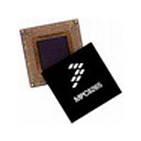
MPC8270CVVUPEA Freescale, MPC8270CVVUPEA Datasheet - Page 78

MPC8270CVVUPEA
Manufacturer Part Number
MPC8270CVVUPEA
Description
Manufacturer
Freescale
Datasheet
1.MPC8270CVVUPEA.pdf
(80 pages)
Specifications of MPC8270CVVUPEA
Family Name
MPC82XX
Device Core
PowerQUICC II
Device Core Size
32b
Frequency (max)
450MHz
Instruction Set Architecture
RISC
Operating Supply Voltage (max)
1.6V
Operating Supply Voltage (min)
1.45V
Operating Temp Range
-40C to 105C
Operating Temperature Classification
Industrial
Mounting
Surface Mount
Pin Count
480
Package Type
TBGA
Lead Free Status / RoHS Status
Compliant
Available stocks
Company
Part Number
Manufacturer
Quantity
Price
Company:
Part Number:
MPC8270CVVUPEA
Manufacturer:
Freescale Semiconductor
Quantity:
135
Company:
Part Number:
MPC8270CVVUPEA
Manufacturer:
FREE
Quantity:
4
Company:
Part Number:
MPC8270CVVUPEA
Manufacturer:
Freescale Semiconductor
Quantity:
10 000
Part Number:
MPC8270CVVUPEA
Manufacturer:
NXP/恩智浦
Quantity:
20 000
Document Revision History
78
Revision
1.0
2/2004
Date
MPC8280 PowerQUICC™ II Family Hardware Specifications, Rev. 1.8
• Removal of “Advance Information” and “Preliminary.” The MPC8280 is fully qualified.
•
•
• Section 1.1: Core frequency range is 166–450 MHz
• Addition of ZQ (516 PBGA with Lead spheres) package references
•
• Note following
•
•
•
•
•
• Sections 4.1–4.5: New
•
•
•
•
• Section 6.2: Addition of Note: CLKIN Jitter and Duty Cycle
•
•
•
•
•
•
•
• Addition of “Note: Temperature Reflow for the VR Package" on page 59
•
•
•
•
•
Table
Figure
Table
Table
Table
Table
Table
Table
Table
Table
Table
Table
Table
Table
Table 16
to corresponding values in tables.
Table
Table
Table
Table
Table
Table
PA6—FCC2_UT_RXADDR3
PA7—FCC2_UT_TXADDR3
PA8—FCC2_UT_TXADDR4
PB14—RXD3
PC19—SPICLK
PC22—FCC1_UT_TXPRTY
PC28—FCC2_UT_RXADDR4
Table
PA[6–9], PB[8–17, 20–25], PC[6–7, 10–13], PD[4, 10–13, 16, 23–28]
Table
Table
Table 25. Document Revision History (continued)
1: New
4: VDD and VCCSYN modified to 1.45–1.60 V
5: Addition of note 2 regarding TRST and PORESET (see VIH row of
5: Changed I
5: Moved QREQ to V
5: Addition of critical interrupt (CINT) to IRQ5 for V
6: Addition of Ψ
7: Modified power values (+ 150mW to each)
8: Addition of note 2. Changed PCI impedance to 27 Ω.
9: Changes to sp36b, SP38a, sp38b, sp37a, sp39a, sp40 and sp41
10: Changes to sp16a, sp18a, sp20 and sp21
11: Changes to sp13 @ 66 and 83 MHz, sp14 @ 83 MHz
12: Change to sp30 (data bus signals). Changes to sp33b. Removal of note 2.
21: Addition of note 1 to TRST (AH3) and PORESET (AG6)
21: Addition of RXD3 to CPM port pin PB14. Previously omitted.
21: Addition of critical interrupt (CINT) to B21 and U4. Previously omitted.
21: Addition of note 5 to ‘No connect’ (AA1, AG4)
23: Addition of note 1 to TRST (F22) and PORESET (B25)
23: Addition of previously omitted signals that are multiplexed with CPM port pins:
23: Removal of serial interface 1 (SI1) signals from port pins (see note 2 in
23: Addition of critical interrupt (CINT) to AC1 and B14. Previously omitted.
23: Addition of note 5 to ‘No connect’ (E17, C23)
1: Modification to note 2
through
Table
Table
OL
4: Modified
JT
for 60x signals to 6.0 mA
20: Modification of note 1 regarding CPU and CPM Fmin. Modification
and note 4
OL
: I
OL
Substantive Changes
= 3.2 mA
OL
(I
OL
= 6.0mA)
Freescale Semiconductor
Table
Figure
5)
1):


