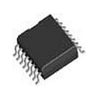
TP3057WM National Semiconductor, TP3057WM Datasheet - Page 6

TP3057WM
Manufacturer Part Number
TP3057WM
Description
Manufacturer
National Semiconductor
Type
PCMr
Datasheet
1.TP3057WM.pdf
(16 pages)
Specifications of TP3057WM
Number Of Channels
1
Gain Control
Adjustable
Number Of Adc's
1
Number Of Dac's
1
Package Type
SOIC W
Operating Supply Voltage (typ)
±5V
Number Of Adc Inputs
1
Number Of Dac Outputs
1
Operating Supply Voltage (max)
±5.25V
Operating Supply Voltage (min)
±4.75V
Operating Temperature (max)
85C
Operating Temperature (min)
-40C
Pin Count
16
Mounting
Surface Mount
Lead Free Status / RoHS Status
Not Compliant
Available stocks
Company
Part Number
Manufacturer
Quantity
Price
Part Number:
TP3057WM
Manufacturer:
NS
Quantity:
20 000
Part Number:
TP3057WMX
Manufacturer:
NS/国半
Quantity:
20 000
Symbol
1 t
t
t
t
t
t
t
t
t
t
t
t
t
t
t
t
t
t
t
t
t
t
t
t
t
RM
FM
PB
RB
FB
WMH
WML
SBFM
SFFM
WBH
WBL
HBFL
HBFS
SFB
DBD
DBTS
DZC
DZF
SDB
HBD
SF
HF
HBFl
WFL
Timing Specifications
5 0V
assured by correlation with other production tests and or product design and characterization All signals referenced to GNDA
Typicals specified at V
0 7V See Definitions and Timing Conventions section for test methods information
PM
g
5% V
Frequency of Master Clocks
Rise Time of Master Clock
Fall Time of Master Clock
Period of Bit Clock
Rise Time of Bit Clock
Fall Time of Bit Clock
Width of Master Clock High
Width of Master Clock Low
Set-Up Time from BCLK
to MCLK
Set-Up Time from FS
to MCLK
Width of Bit Clock High
Width of Bit Clock Low
Holding Time from Bit Clock
Low to Frame Sync
Holding Time from Bit Clock
High to Frame Sync
Set-Up Time from Frame Sync
to Bit Clock Low
Delay Time from BCLK
to Data Valid
Delay Time to TS
Delay Time from BCLK
Data Output Disabled
Delay Time to Valid Data from
FS
Comes Later
Set-Up Time from D
BCLK
Hold Time from BCLK
D
Set-Up Time from FS
BCLK
Hold Time from BCLK
to FS
Hold Time from 3rd Period of
Bit Clock Low to Frame Sync
(FS
Minimum Width of the Frame
Sync Pulse (Low Level)
R
BB
X
Invalid
X
or BCLK
e b
X R
or FS
R X
X R
X
X
Low
Low
Low
5 0V
Falling Edge
Falling Edge
Parameter
R
CC
)
X
e
Whichever
g
5 0V V
X
5% T
Low
R
X
X R
Valid to
R X
X R
High
X
X
A
X
BB
High
Low to
to
e
Unless otherwise noted limits printed in BOLD characters are guaranteed for V
High
Low to
Low
e b
0 C to 70 C by correlation with 100% electrical testing at T
5 0V T
Depends on the Device Used and the
BCLK
MCLK
MCLK
MCLK
BCLK
BCLK
MCLK
MCLK
First Bit Clock after the Leading
Edge of FS
Long Frame Only
V
V
Long Frame Only
Short Frame Only
Long Frame Only
Load
Load
C
C
Short Frame Sync Pulse (1 Bit Clock
Period Long)
Short Frame Sync Pulse (1 Bit Clock
Period Long)
Long Frame Sync Pulse (from 3 to 8 Bit
Clock Periods Long)
64k Bit s Operating Mode
IH
IL
L
L
A
e
e
e
e
e
0 pF to 150 pF
0 pF to 150 pF
e
e
0 6V
2 2V
R
X
X
X
X
X
X
X
150 pF plus 2 LSTTL Loads
150 pF plus 2 LSTTL Loads
25 C All timing parameters are measured at V
and BCLK
and BCLK
and MCLK
and MCLK
and MCLK
and MCLK
and MCLK
CLKSEL Pin
X
Conditions
6
R
R
R
R
R
R
R
160
160
100
100
160
160
100
100
160
Min
485
80
50
50
50
50
20
0
0
0
A
e
2 048
1 536
1 544
OH
488
Typ
25 C All other limits are
e
2 0V and V
15725
Max
140
140
165
165
50
50
50
50
CC
OL
e
e
Units
MHz
MHz
MHz
ns
ns
ns
ns
ns
ns
ns
ns
ns
ns
ns
ns
ns
ns
ns
ns
ns
ns
ns
ns
ns
ns
ns
ns


