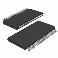
ICS9FG107AGLNT IDT, Integrated Device Technology Inc, ICS9FG107AGLNT Datasheet - Page 10

ICS9FG107AGLNT
Manufacturer Part Number
ICS9FG107AGLNT
Description
IC FREQ TIMING GENERATOR 48TTSOP
Manufacturer
IDT, Integrated Device Technology Inc
Type
Frequency Generatorr
Datasheet
1.ICS9FG107AGLNT.pdf
(18 pages)
Specifications of ICS9FG107AGLNT
Input
Clock, Crystal
Output
Clock
Frequency - Max
400MHz
Voltage - Supply
3.135 V ~ 3.465 V
Operating Temperature
0°C ~ 70°C
Mounting Type
Surface Mount
Package / Case
48-TSSOP
Frequency-max
400MHz
Lead Free Status / RoHS Status
Lead free / RoHS Compliant
Other names
9FG107AGLNT
Absolute Max
Electrical Characteristics - Input/Supply/Common Output Parameters
IDT
T
Operating Supply Current
Input Rise and Fall times
1
2
3
Tambient
ESD prot
ppm frequency accuracy on PLL outputs.
Guaranteed by design and characterization, not 100% tested in production.
See timing diagrams for timing requirements.
Symbol
VDD_In
VDD_A
A
Input frequency should be measured at the REFOUT pin and tuned to ideal 14.31818MHz or 25 MHz to meet
Modulation Frequency
Tcase
ICS9FG107
Programmable FTG for Differential P4
TM
= 0 - 70°C; Supply Voltage V
Input High Voltage
Clk Stabilization
Input High Current
Input Low Voltage
DIF output enable
Ts
Input Low Current
Input Frequency
/ICS
Pin Inductance
PARAMETER
Capacitance
Input/Output
TM
Programmable FTG for Differential P4
3.3V Logic Input Supply Voltage
3.3V Core Supply Voltage
Ambient Operating Temp
Storage Temperature
Input ESD protection
human body model
1
Case Temperature
1,2
1
3
Parameter
SYMBOL
I
DD3.3OP
T
t
C
f
DIFOE
t
V
L
C
V
I
I
MOD
STAB
R
I
F
IL1
IL2
OUT
IH
pin
/t
DD
IH
IN
IL
i
F
= 3.3 V +/-5%
TM
TM
input clock stabilization to 1st
V
From V
V
IN
Full Active, C
Full Active, C
CPU, PCI-Express & SATA Clocks
IN
CPU, PCI-Express & SATA Clocks
DIF_Stop# de-assertion
Output pin capacitance
DIF output enable after
= 0 V; Inputs with no pull-
= 0 V; Inputs with pull-up
Triangular Modulation
20% to 80% of VDD
GND - 0.5
DD
CONDITIONS
f = 400 MHz
f = 100 MHz
Logic Inputs
3.3 V +/-5%
3.3 V +/-5%
up resistors
V
2000
Min
-65
V
Power-Up and after
resistors
DD
0
IN
clock
= 3.3 V
= V
L
L
= Full load;
= Full load;
DD
V
V
10
DD
DD
Max
150
115
+ 0.5V
+ 0.5V
70
V
SS
MIN
-200
1.5
14
30
-5
-5
2
Units
- 0.3
°
°C
°C
V
V
V
C
TYP
V
DD
ICS9FG107
MAX
250
200
0.8
1.8
25
40
10
5
7
5
6
5
+ 0.3
UNITS NOTES
MHz
kHz
mA
mA
ms
uA
uA
uA
nH
pF
pF
ns
ns
V
V
REV F 08/21/07
1,2
3
1
1
1
1
1
1


