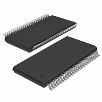
ICS9FG107AGLNT IDT, Integrated Device Technology Inc, ICS9FG107AGLNT Datasheet

ICS9FG107AGLNT
Specifications of ICS9FG107AGLNT
Related parts for ICS9FG107AGLNT
ICS9FG107AGLNT Summary of contents
Page 1
Programmable FTG for Differential P4 Clocks Description ICS9FG107 is a Frequency Timing Generator that provides 7 differential output pairs that are compliant to the Intel CK409/CK410 specification. It provides support for PCI-Express, next generation I/ O, and SATA. The part ...
Page 2
ICS9FG107 Programmable FTG for Differential P4 Pin Configuration XIN/CLKIN VDD 3 GND 4 FS2/REFOUT* 5 GND 6 FS0/PCICLK_F* 7 PCICLK0 8 PCICLK1 9 VDD 10 OE_6** 11 DIF_6 12 DIF_6# 13 VDD 14 GND 15 OE_5** 16 ...
Page 3
ICS9FG107 Programmable FTG for Differential P4 Pin Description PIN # PIN NAME 1 XIN/CLKIN VDD 4 GND 5 FS2/REFOUT* 6 GND 7 FS0/PCICLK_F* 8 PCICLK0 9 PCICLK1 10 VDD 11 OE_6** 12 DIF_6 13 DIF_6# 14 VDD ...
Page 4
ICS9FG107 Programmable FTG for Differential P4 Pin Description (Continued) PIN # PIN NAME 25 DIF_STOP# 26 SPREAD* 27 SEL14M_25M#** 28 OE_3* 29 DIF_3# 30 DIF_3 31 VDD DIF_2 DIF_2 34 OE_2** 35 GND 36 VDD 37 OE_1** 38 ...
Page 5
ICS9FG107 Programmable FTG for Differential P4 General SMBus serial interface information for the ICS9FG107 How to Write: • Controller (host) sends a start bit. • Controller (host) sends the write address DC • ICS clock will acknowledge • Controller (host) ...
Page 6
ICS9FG107 Programmable FTG for Differential Table: Device Control Register, READ/WRITE ADDRESS (DC/DD) Byte 0 Pin # 27 Bit 7 5 Bit 6 44 Bit 5 Bit Bit 3 Enable Software Control of Frequency, ...
Page 7
ICS9FG107 Programmable FTG for Differential Table: Frequency Select Readback Register Byte 3 Pin # SEL14M_25M# 27 Bit 7 5 Bit 6 44 Bit 5 7 Bit 4 26 Bit 3 Bit 2 Bit 1 45 Bit ...
Page 8
ICS9FG107 Programmable FTG for Differential Table: Byte Count Register Byte 6 Pin # Bit Bit 6 - Bit 5 - Bit 4 Bit 3 - Bit 2 - Bit Bit ...
Page 9
ICS9FG107 Programmable FTG for Differential P4 DIF_STOP# - Assertion (transition from '1' to '0') Asserting DIF_STOP# pin stops all DIF outputs that are set to be stoppable after their next transition. When the SMBus DIF_STOP tri-state bit corresponding to the ...
Page 10
ICS9FG107 Programmable FTG for Differential P4 Absolute Max Symbol Parameter VDD_A 3.3V Core Supply Voltage VDD_In 3.3V Logic Input Supply Voltage Ts Storage Temperature Tambient Ambient Operating Temp Tcase Case Temperature Input ESD protection human body model ESD prot Electrical ...
Page 11
ICS9FG107 Programmable FTG for Differential P4 Electrical Characteristics - DIF 0.7V Current Mode Differential Pair 70° 3.3 V +/-5%; C =2pF PARAMETER SYMBOL Current Source Output Impedance Voltage High Voltage ...
Page 12
ICS9FG107 Programmable FTG for Differential P4 Output-Output Skew (DIFF0 as REFERENCE) Window Skew Skew (ps) Dif0:1 Dif0:2 Dif0:3 Dif0:4 Dif0:5 Dif0:6 1 Guaranteed by design and characterization, not 100% tested in production. Output-Output Skew (DIFF3 as REFERENCE) Window Skew Skew ...
Page 13
ICS9FG107 Programmable FTG for Differential P4 Electrical Characteristics - PCICLK/PCICLK_F 70° 3.3 V +/-5 PARAMETER SYMBOL Long Accuracy ppm Clock period T period Absolute Min/Max Clock T abs period Clk ...
Page 14
ICS9FG107 Programmable FTG for Differential P4 Common Recommendations for Differential Routing L1 length, Route as non-coupled 50 ohm trace. L2 length, Route as non-coupled 50 ohm trace. L3 length, Route as non-coupled 50 ohm trace Down Device Differential ...
Page 15
ICS9FG107 Programmable FTG for Differential P4 Alternative termination for LVDS and other common differential signals. Vdiff Vp-p Vcm 0.45 v 0.22v 1.08 0.58 0.28 0.6 0.80 0.40 0.6 0.60 0.3 1.2 R1a = R1b = R1 Figure_3. L1 L1’ HSCL ...
Page 16
ICS9FG107 Programmable FTG for Differential INDEX INDEX AREA AREA Ordering Information ICS 9FG107yFLFT Example: ICS XXXX IDT /ICS Programmable FTG for Differential P4 TM ...
Page 17
ICS9FG107 Programmable FTG for Differential INDEX INDEX AREA AREA Ordering Information ICS 9FG107yGLFT Example: ICS XXXX IDT /ICS Programmable FTG for Differential ...
Page 18
ICS9FG107 Programmable FTG for Differential P4 Revision History Rev. Issue Date Description D 08/06/07 Updated Differential Output Skew Specifications E 08/08/07 Updated Differential Output Skew Specifications F 08/21/07 Updated Differential Output Skew Specifications TM TM CPU, PCI-Express & SATA Clocks ...


