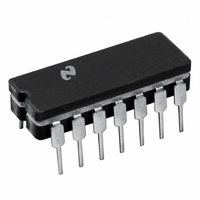
DS0026CJ National Semiconductor, DS0026CJ Datasheet - Page 7

DS0026CJ
Manufacturer Part Number
DS0026CJ
Description
IC CLOCK DRIVER DUAL 5MHZ 14CDIP
Manufacturer
National Semiconductor
Type
Fanout Buffer (Distribution)r
Datasheet
1.DS0026CN.pdf
(12 pages)
Specifications of DS0026CJ
Number Of Circuits
1
Ratio - Input:output
2:2
Differential - Input:output
No/No
Input
TTL
Output
MOS
Frequency - Max
10MHz
Operating Temperature
0°C ~ 70°C
Mounting Type
Through Hole
Package / Case
14-CDIP (0.300", 7.62mm)
Frequency-max
10MHz
Lead Free Status / RoHS Status
Contains lead / RoHS non-compliant
Voltage - Supply
-
Other names
*DS0026CJ
Available stocks
Company
Part Number
Manufacturer
Quantity
Price
Company:
Part Number:
DS0026CJ
Manufacturer:
NS
Quantity:
2 445
Company:
Part Number:
DS0026CJ
Manufacturer:
HARRIS
Quantity:
2 450
Part Number:
DS0026CJ
Manufacturer:
NS/国半
Quantity:
20 000
Company:
Part Number:
DS0026CJ-8
Manufacturer:
MOT
Quantity:
400
Part Number:
DS0026CJ-8
Manufacturer:
NS/国半
Quantity:
20 000
Limiting the inductance of the clock lines can be accom-
plished by minimizing their length and by laying out the lines
such that the return current is closely coupled to the clock
lines. When minimizing the length of clock lines it is important
to minimize the distance from the clock driver output to the
furthest point being driven. Because of this, memory boards
are usually designed with clock drivers in the center of the
memory array, rather than on one side, reducing the maxi-
mum distance by a factor of 2.
Using multilayer printed circuit boards with clock lines sand-
wiched between the V
inductance of the clock lines. It also serves the function of
preventing the clocks from coupling noise into input and out-
put lines. Unfortunately multilayer printed circuit boards are
more expensive than two sided boards. The user must make
the decision as to the necessity of multilayer boards. Suffice
it to say here, that reliable memory boards can be designed
using two sided printed circuit boards.
FIGURE 4. Clock Waveforms (Voltage and Current)
DD
and V
SS
power plains minimizes the
5853 Version 6 Revision 3
585319
Print Date/Time: 2010/07/13 22:49:07
7
Because of the amount of current that the clock driver must
supply to its capacitive load, the distribution of power to the
clock driver must be considered.
voltage and current waveforms for a clock driver driving a
1000 pF capacitor with 20 ns rise and fall time.
As can be seen the current is significant. This current flows in
the V
lines will produce large voltage transients on the power sup-
plies. A bypass capacitor, as close as possible to the clock
driver, is helpful in minimizing this problem. This bypass is
most effective when connected between the V
supplies. The size of the bypass capacitor depends on the
amount of capacitance being driven. Using a low inductance
capacitor, such as a ceramic or silver mica, is most effective.
Another helpful technique is to run the V
the clock driver, adjacent to each other. This tends to reduce
the lines inductance and therefore the magnitude of the volt-
age transients.
While discussing the clock driver, it should be pointed out that
the DS0026 is a relatively low input impedance device. It is
possible to couple current noise into the input without seeing
a significant voltage. Since the noise is difficult to detect with
an oscilloscope it is often overlooked.
DD
and V
SS
power lines. Any significant inductance in the
Figure 4
DD
gives the idealized
and V
www.national.com
SS
SS
and V
lines, to
DD


