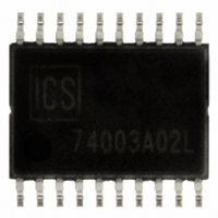
ICS874003AG-02LF IDT, Integrated Device Technology Inc, ICS874003AG-02LF Datasheet

ICS874003AG-02LF
Specifications of ICS874003AG-02LF
800-1214-5
800-1214
874003AG-02LF
Related parts for ICS874003AG-02LF
ICS874003AG-02LF Summary of contents
Page 1
... ICS874003AG-02 REVISION B SEPTEMBER 14, 2010 Features • Three differential LVDS output pairs • One differential clock input • CLK, nCLK supports the following input levels: LVPECL, LVDS, LVHSTL, HCSL, SSTL • Input frequency range: 98MHz to 128MHz • Output frequency range: 98MHz to 320MHz • ...
Page 2
... ICS874003-02 Data Sheet Block Diagram Pullup OEA 3 Pulldown F_SEL2:0 Pulldown CLK Phase Pullup Detector nCLK Pulldown MR ICS874003AG-02 REVISION B SEPTEMBER 14, 2010 VCO 490 - 640MHz M = ÷5 (fixed) 2 PCI EXPRESS™ JITTER ATTENUATOR QA0 ÷5 ÷4 nQA0 ÷2 (default) QA1 nQA1 3 QB0 ÷5 ÷4 ÷ ...
Page 3
... QA[0:1], nQA[0: Hi-Impedance 1 1 Enabled ICS874003AG-02 REVISION B SEPTEMBER 14, 2010 Type Description Differential output pair. LVDS interface levels. Output supply pins. Differential output pair. LVDS interface levels. Active HIGH Master Reset. When logic HIGH, the internal dividers are reset causing the true outputs (Qx low and the inverted outputs (nQx high. ...
Page 4
... IH V Input Low Voltage IL OEA, OEB I Input High Current F_SEL0, F_SEL1, IH F_SEL2, MR OEA, OEB I Input Low Current F_SEL0, F_SEL1, IL F_SEL2, MR ICS874003AG-02 REVISION B SEPTEMBER 14, 2010 Rating 4.6V -0. 0.5V DD 10mA 15mA 73.2°C/W (0 lfpm) -65°C to 150° 3.3V ± 5 DDA DDO Test Conditions ...
Page 5
... NOTE 2: Defined as skew between outputs at the same supply voltage and with equal load conditions. Measured at the differential cross points. NOTE 3: These parameters are guaranteed by characterization. Not tested in production. NOTE 4: Defined as skew within a bank of outputs at the same voltage and with equal load conditions. ICS874003AG-02 REVISION B SEPTEMBER 14, 2010 = 3.3V ± 5%, T ...
Page 6
... V DDA 3.3V LVDS Output Load AC Test Circuit nQA0 QA0 nQA1 QA1 tsk(b) Bank Skew nQx Qx nQy Qy tsk(o) Output Skew ICS874003AG-02 REVISION B SEPTEMBER 14, 2010 V DD SCOPE nCLK Qx CLK nQx GND Differential Input Level nQA[0:1], nQB0 QA[0:1], QB0 Cycle-to-Cycle Jitter nQA[0:1], nQB0 ...
Page 7
... ICS874003-02 Data Sheet Parameter Measurement Information, continued nQA[0:1], nQB0 80% QA[0:1], 20% QB0 t R Output Rise/Fall Time V DD LVDS DC Input Differential Output Voltage Setup ICS874003AG-02 REVISION B SEPTEMBER 14, 2010 80 Input 20 Offset Voltage Setup out ➤ 100 V /∆ ➤ out 7 PCI EXPRESS™ JITTER ATTENUATOR ...
Page 8
... In addition, matched termination at the input will attenuate the signal in half. This can be done in one of two ways. First, R3 and R4 in parallel should equal the transmission Figure 1. Recommended Schematic for Wiring a Differential Input to Accept Single-ended Levels ICS874003AG-02 REVISION B SEPTEMBER 14, 2010 and V should be DDO DDA line impedance. For most 50Ω ...
Page 9
... R3 and R4 can be 0Ω Figure 3E. CLK/nCLK Input Driven by a 3.3V HCSL Driver ICS874003AG-02 REVISION B SEPTEMBER 14, 2010 Please consult with the vendor of the driver component to confirm the driver termination requirements. For example, in Figure 3A, the input PP termination applies for IDT open emitter LVHSTL drivers. If you are using an LVHSTL driver from another vendor, use their termination recommendation ...
Page 10
... The standard LVDS Driver 100Ω Differential Transmission Line Figure 4. Typical LVDS Driver Termination ICS874003AG-02 REVISION B SEPTEMBER 14, 2010 Outputs: LVDS Outputs All unused LVDS output pairs can be either left floating or terminated with 100Ω across. If they are left floating, there should be no trace attached ...
Page 11
... Linear Feet per Minute Single-Layer PCB, JEDEC Standard Test Boards Multi-Layer PCB, JEDEC Standard Test Boards NOTE: Most modern PCB designs use multi-layered boards. The data in the second row pertains to most designs. ICS874003AG-02 REVISION B SEPTEMBER 14, 2010 = 3. 3.465V, which gives worst case results ...
Page 12
... NOTE: Most modern PCB designs use multi-layered boards. The data in the second row pertains to most designs. Transistor Count The transistor count for ICS874003-02 is: 1408 Package Outline and Package Dimensions Package Outline - G Suffix for 20 Lead TSSOP ICS874003AG-02 REVISION B SEPTEMBER 14, 2010 θ by Velocity JA 0 200 114.5° ...
Page 13
... Any other applications, such as those requiring extended temperature ranges, high reliability or other extraordinary environmental requirements are not recommended without additional processing by IDT. IDT reserves the right to change any circuitry or specifications without notice. IDT does not authorize or warrant any IDT product for use in life support devices or critical medical instruments. ICS874003AG-02 REVISION B SEPTEMBER 14, 2010 Package Shipping Packaging ...
Page 14
... Updated Differential Clock Input Interface. 9 Updated LVDS Driver Termination. 10 Ordering Information Table - deleted "ICS" prefix in Part/Order column, added "ICS" prefix 13 to marking column. Converted datasheet format. ICS874003AG-02 REVISION B SEPTEMBER 14, 2010 (nCLK) spec from 5uA min to 5uA max. Corrected PCI EXPRESS™ JITTER ATTENUATOR Date /I rows. ...
Page 15
ICS874003-04 Data Sheet We’ve Got Your Timing Solution 6024 Silver Creek Valley Road Sales 800-345-7015 (inside USA) San Jose, California 95138 +408-284-8200 (outside USA) Fax: 408-284-2775 www.IDT.com/go/contactIDT DISCLAIMER Integrated Device Technology, Inc. (IDT) and its subsidiaries reserve the right to ...


