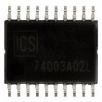
ICS874003AG-02LF IDT, Integrated Device Technology Inc, ICS874003AG-02LF Datasheet - Page 10

ICS874003AG-02LF
Manufacturer Part Number
ICS874003AG-02LF
Description
IC JITTER ATTENUATOR 20-TSSOP
Manufacturer
IDT, Integrated Device Technology Inc
Series
HiPerClockS™r
Type
Jitter Attenuatorr
Datasheet
1.ICS874003AG-02LF.pdf
(15 pages)
Specifications of ICS874003AG-02LF
Input
HCSL, LVDS, LVHSTL, LVPECL, SSTL
Output
LVDS
Frequency - Max
320MHz
Voltage - Supply
3.135 V ~ 3.465 V
Operating Temperature
0°C ~ 70°C
Mounting Type
Surface Mount
Package / Case
20-TSSOP
Frequency-max
320MHz
Number Of Elements
1
Supply Current
75mA
Pll Input Freq (min)
98MHz
Pll Input Freq (max)
128MHz
Operating Supply Voltage (typ)
3.3V
Operating Temp Range
0C to 70C
Package Type
TSSOP
Output Frequency Range
98 to 320MHz
Operating Supply Voltage (min)
3.015/3.135V
Operating Supply Voltage (max)
3.465V
Operating Temperature Classification
Commercial
Pin Count
20
Lead Free Status / RoHS Status
Lead free / RoHS Compliant
Other names
800-1214
800-1214-5
800-1214
874003AG-02LF
800-1214-5
800-1214
874003AG-02LF
ICS874003-02 Data Sheet
Recommendations for Unused Input and Output Pins
Inputs:
LVCMOS Control Pins
All control pins have internal pullups or pulldowns; additional
resistance is not required but can be added for additional protection.
A 1kΩ resistor can be used.
LVDS Driver Termination
A general LVDS interface is shown in Figure 4. Standard termination
for LVDS type output structure requires both a 100Ω parallel resistor
at the receiver and a 100Ω differential transmission line environment.
In order to avoid any transmission line reflection issues, the 100Ω
resistor must be placed as close to the receiver as possible. IDT
offers a full line of LVDS compliant devices with two types of output
structures: current source and voltage source. The standard
Figure 4. Typical LVDS Driver Termination
ICS874003AG-02 REVISION B SEPTEMBER 14, 2010
LVDS Driver
100Ω Differential Transmission Line
100Ω
10
Outputs:
LVDS Outputs
All unused LVDS output pairs can be either left floating or terminated
with 100Ω across. If they are left floating, there should be no trace
attached.
termination schematic as shown in Figure 4 can be used with either
type of output structure. If using a non-standard termination, it is
recommended to contact IDT and confirm if the output is a current
source or a voltage source type structure. In addition, since these
outputs are LVDS compatible, the amplitude and common mode
input range of the input receivers should be verified for compatibility
with the output.
+
–
LVDS
Receiver
©2010 Integrated Device Technology, Inc.
PCI EXPRESS™ JITTER ATTENUATOR


