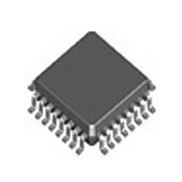
ICS8624BYLF IDT, Integrated Device Technology Inc, ICS8624BYLF Datasheet - Page 13

ICS8624BYLF
Manufacturer Part Number
ICS8624BYLF
Description
IC BUFFER ZD 1-5 HSTL 32-LQFP
Manufacturer
IDT, Integrated Device Technology Inc
Series
HiPerClockS™r
Type
Fanout Distribution, Multiplexer , Zero Delay Bufferr
Datasheet
1.ICS8624BYLFT.pdf
(19 pages)
Specifications of ICS8624BYLF
Pll
Yes with Bypass
Input
HCSL, LVDS, LVHSTL, LVPECL, SSTL
Output
HSTL
Number Of Circuits
1
Ratio - Input:output
2:5
Differential - Input:output
Yes/Yes
Frequency - Max
700MHz
Divider/multiplier
Yes/No
Voltage - Supply
3.135 V ~ 3.465 V
Operating Temperature
0°C ~ 70°C
Mounting Type
Surface Mount
Package / Case
32-LQFP
Frequency-max
700MHz
Number Of Elements
1
Supply Current
120mA
Pll Input Freq (min)
31.25MHz
Pll Input Freq (max)
700MHz
Operating Supply Voltage (typ)
3.3V
Operating Temp Range
0C to 70C
Package Type
LQFP
Output Frequency Range
Up to 700MHz
Operating Supply Voltage (min)
3.135V
Operating Supply Voltage (max)
3.465V
Operating Temperature Classification
Commercial
Pin Count
32
Lead Free Status / RoHS Status
Lead free / RoHS Compliant
Other names
8624BYLF
Available stocks
Company
Part Number
Manufacturer
Quantity
Price
Company:
Part Number:
ICS8624BYLF
Manufacturer:
IDT, Integrated Device Technology Inc
Quantity:
10 000
Part Number:
ICS8624BYLF
Manufacturer:
ICS
Quantity:
20 000
Company:
Part Number:
ICS8624BYLFT
Manufacturer:
IDT, Integrated Device Technology Inc
Quantity:
10 000
ICS8624 Data Sheet
Power Considerations
This section provides information on power dissipation and junction temperature for the ICS8624.
Equations and example calculations are also provided.
1.
The total power dissipation for the ICS8624 is the sum of the core power plus the power dissipated in the load(s).
The following is the power dissipation for V
NOTE: Please refer to Section 3 for details on calculating power dissipated in the load.
Total Power_
2. Junction Temperature.
Junction temperature, Tj, is the temperature at the junction of the bond wire and bond pad and directly affects the reliability of the device. The
maximum recommended junction temperature for HiPerClockS devices is 125°C. Limiting the internal transistor junction temperature, Tj, to
125°C ensures that the bond wire and bond pad temperature remains below 125°C.
In order to calculate junction temperature, the appropriate junction-to-ambient thermal resistance θ
a multi-layer board, the appropriate value is 47.9°C/W per Table 7 below.
Therefore, Tj for an ambient temperature of 70°C with all outputs switching is:
This calculation is only an example. Tj will obviously vary depending on the number of loaded outputs, supply voltage, air flow and the type of
board (multi-layer).
Table 7. Thermal Resistance
ICS8624BY REVISION E OCTOBER 6, 2009
Linear Feet per Minute
Multi-Layer PCB, JEDEC Standard Test Boards
Power Dissipation.
•
•
Power (core)
Power (outputs)
If all outputs are loaded, the total power is 5 * 32.8mW = 164mW
The equation for Tj is as follows: Tj = θ
Tj = Junction Temperature
θ
Pd_total = Total Device Power Dissipation (example calculation is in section 1 above)
T
70°C + 0.632W * 47.9°C/W = 100.3°C. This is well below the limit of 125°C.
JA
A
= Ambient Temperature
= Junction-to-Ambient Thermal Resistance
MAX
(3.465V, with all outputs switching) = 467.775mW + 164mW = 631.775mW
MAX
MAX
= V
= 32.8mW/Loaded Output pair
DD_MAX
θ
JA
* (I
for 32 Lead LQFP, Forced Convection
DD_MAX
DD
= 3.3V + 5% = 3.465V, which gives worst case results.
JA
+ I
* Pd_total + T
DDA_MAX
)= 3.465V * (120mA + 15mA) = 467.775mW
θ
JA
A
47.9°C/W
vs. Air Flow
0
13
LOW SKEW, 1-TO-5 DIFFERENTIAL-TO-HSTL ZERO DELAY BUFFER
42.1°C/W
200
JA
must be used. Assuming no air flow and
©2009 Integrated Device Technology, Inc.
39.4°C/W
500


