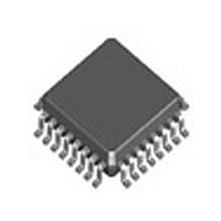
ICS8624BYLF IDT, Integrated Device Technology Inc, ICS8624BYLF Datasheet - Page 9

ICS8624BYLF
Manufacturer Part Number
ICS8624BYLF
Description
IC BUFFER ZD 1-5 HSTL 32-LQFP
Manufacturer
IDT, Integrated Device Technology Inc
Series
HiPerClockS™r
Type
Fanout Distribution, Multiplexer , Zero Delay Bufferr
Datasheet
1.ICS8624BYLFT.pdf
(19 pages)
Specifications of ICS8624BYLF
Pll
Yes with Bypass
Input
HCSL, LVDS, LVHSTL, LVPECL, SSTL
Output
HSTL
Number Of Circuits
1
Ratio - Input:output
2:5
Differential - Input:output
Yes/Yes
Frequency - Max
700MHz
Divider/multiplier
Yes/No
Voltage - Supply
3.135 V ~ 3.465 V
Operating Temperature
0°C ~ 70°C
Mounting Type
Surface Mount
Package / Case
32-LQFP
Frequency-max
700MHz
Number Of Elements
1
Supply Current
120mA
Pll Input Freq (min)
31.25MHz
Pll Input Freq (max)
700MHz
Operating Supply Voltage (typ)
3.3V
Operating Temp Range
0C to 70C
Package Type
LQFP
Output Frequency Range
Up to 700MHz
Operating Supply Voltage (min)
3.135V
Operating Supply Voltage (max)
3.465V
Operating Temperature Classification
Commercial
Pin Count
32
Lead Free Status / RoHS Status
Lead free / RoHS Compliant
Other names
8624BYLF
Available stocks
Company
Part Number
Manufacturer
Quantity
Price
Company:
Part Number:
ICS8624BYLF
Manufacturer:
IDT, Integrated Device Technology Inc
Quantity:
10 000
Part Number:
ICS8624BYLF
Manufacturer:
ICS
Quantity:
20 000
Company:
Part Number:
ICS8624BYLFT
Manufacturer:
IDT, Integrated Device Technology Inc
Quantity:
10 000
ICS8624 Data Sheet
Recommendations for Unused Input and Output Pins
Inputs:
LVCMOS Control Pins
All control pins have internal pullups or pulldowns; additional
resistance is not required but can be added for additional protection.
A 1kΩ resistor can be used.
CLK/nCLK Inputs
For applications not requiring the use of the differential input, both
CLK and nCLK can be left floating. Though not required, but for
additional protection, a 1kΩ resistor can be tied from CLK to ground.
Wiring the Differential Input to Accept Single Ended Levels
Figure 2 shows how the differential input can be wired to accept
single ended levels. The reference voltage V_REF = V
generated by the bias resistors R1, R2 and C1. This bias circuit
should be located as close as possible to the input pin. The ratio of
R1 and R2 might need to be adjusted to position the V_REF in the
center of the input voltage swing. For example, if the input clock swing
is only 2.5V and V
0.609.
ICS8624BY REVISION E OCTOBER 6, 2009
DD
= 3.3V, V_REF should be 1.25V and R2/R1 =
DD
/2 is
9
Outputs:
HSTL Outputs
All unused HSTL outputs can be left floating. We recommend that
there is no trace attached. Both sides of the differential output pair
should either be left floating or terminated.
Figure 2. Single-Ended Signal Driving Differential Input
LOW SKEW, 1-TO-5 DIFFERENTIAL-TO-HSTL ZERO DELAY BUFFER
CLK_IN
0.1uF
C1
R1
1K
V_REF
R2
1K
©2009 Integrated Device Technology, Inc.
V
DD
CLKx
nCLKx


