ICS8624BYLF IDT, Integrated Device Technology Inc, ICS8624BYLF Datasheet
ICS8624BYLF
Specifications of ICS8624BYLF
Available stocks


Related parts for ICS8624BYLF


ICS8624BYLF Summary of contents
Page 1
Low Skew, 1-to-5 Differential-to-HSTL Zero Delay Buffer General Description The ICS8624 is a high performance, 1-to-5 ICS Differential-to-HSTL zero delay buffer and a member of the HiPerClockS™ family of High Performance HiPerClockS™ Clock Solutions from IDT. The ICS8624 has two ...
Page 2
ICS8624 Data Sheet Table 1. Pin Descriptions Number Name 1, 2 SEL0, SEL1 Input 3 CLK0 Input 4 nCLK0 Input 5 CLK1 Input 6 nCLK1 Input 7 CLK_SEL Input 8 MR Input Power DD 10 nFB_IN Input ...
Page 3
ICS8624 Data Sheet Function Tables Table 3A. Control Input Function Table Inputs SEL1 SEL0 Reference Frequency Range (MHz *NOTE: VCO frequency range for all configurations above is 250MHz to 700MHz. Table 3B. ...
Page 4
ICS8624 Data Sheet Absolute Maximum Ratings NOTE: Stresses beyond those listed under Absolute Maximum Ratings may cause permanent damage to the device. These ratings are stress specifications only. Functional operation of product at these conditions or any conditions beyond those ...
Page 5
ICS8624 Data Sheet Table 4C. Differential DC Characteristics, V Symbol Parameter FB_IN, CLK0, CLK1 I Input High Current IH nFB_IN, nCLK0, nCLK1 FB_IN, CLK0, CLK1 I Input Low Current IL nFB_IN, nCLK0, nCLK1 V Peak-to-Peak Voltage; NOTE ...
Page 6
ICS8624 Data Sheet AC Electrical Characteristics Table 6A. AC Characteristics, V Symbol Parameter f Output Frequency MAX t Propagation Delay; NOTE 1 PD t(Ø) Static Phase Offset; NOTE 2, 5 tsk(o) Output Skew; NOTE 3, 5 tjit(cc) Cycle-to-Cycle Jitter; NOTE ...
Page 7
ICS8624 Data Sheet Parameter Measurement Information 3.3V±5% 1.8V±0.2V V DD, V DDA V DDO HSTL GND 0V 3.3V Core/1.8V Output Load AC Test Circuit nCLK0, nCLK1 CLK0, CLK1 nFB_IN FB_IN ➤ ➤ t(Ø) tjit(Ø) = t(Ø) – t(Ø) t(Ø) ...
Page 8
ICS8624 Data Sheet Parameter Measurement Information, continued nQ[0:4] 80 20% Q[0: Output Rise/Fall Time Application Information Power Supply Filtering Technique To achieve optimum jitter performance, power supply isolation is required. To achieve optimum jitter performance, power ...
Page 9
ICS8624 Data Sheet Recommendations for Unused Input and Output Pins Inputs: LVCMOS Control Pins All control pins have internal pullups or pulldowns; additional resistance is not required but can be added for additional protection. A 1kΩ resistor can be used. ...
Page 10
ICS8624 Data Sheet Differential Clock Input Interface The CLK /nCLK accepts LVDS, LVPECL, LVHSTL, SSTL, HCSL and other differential signals. Both signals must meet the V input requirements. Figures show interface examples for the HiPerClockS CLK/nCLK input ...
Page 11
ICS8624 Data Sheet Schematic Example The schematic of the ICS8624 layout example is shown in Figure 4A. The ICS8624 recommended PCB board layout for this example is shown in Figure 4B. This layout example is used as a general VDD ...
Page 12
ICS8624 Data Sheet The following component footprints are used in this layout example: All the resistors and capacitors are size 0603. Power and Grounding Place the decoupling capacitors C1, C6, C2, C4, and C5, as close as possible to the ...
Page 13
ICS8624 Data Sheet Power Considerations This section provides information on power dissipation and junction temperature for the ICS8624. Equations and example calculations are also provided. 1. Power Dissipation. The total power dissipation for the ICS8624 is the sum of the ...
Page 14
ICS8624 Data Sheet 3. Calculations and Equations. The purpose of this section is to calculate the power dissipation for the HSTL output pairs. HSTL output driver circuit and termination are shown in Figure 5. V DDO Q1 Figure 5. HSTL ...
Page 15
ICS8624 Data Sheet Reliability Information θ Table 8. vs. Air Flow Table for a 32 Lead LQFP JA Linear Feet per Minute Multi-Layer PCB, JEDEC Standard Test Boards Transistor Count The transistor count for ICS8624 is: 1565 ICS8624BY REVISION E ...
Page 16
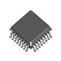
ICS8624 Data Sheet Package Outline and Dimensions Package Outline - Y Suffix for 32 Lead LQFP Table 9. Package Dimensions for 32 Lead LQFP JEDEC Variation: BBA All Dimensions in Millimeters Symbol Minimum Nominal 0.05 A2 ...
Page 17
... ICS8624BYLF 8624BYLFT ICS8624BYLF NOTE: Parts that are ordered with an "LF" suffix to the part number are the Pb-Free configuration and are RoHS compliant. While the information presented herein has been checked for both accuracy and reliability, Integrated Device Technology (IDT) assumes no responsibility for either its use or for the infringement of any patents or other rights of third parties, which would result from its use ...
Page 18
ICS8624 Data Sheet Revision History Sheet Rev Table Page Description of Change 8 Switched labels on Figure 8, odc & Revised label on Figure 11 to read ICS8624 LVHSTL... from ICS8634 LVDS... A 1 Revised Block Diagram. ...
Page 19
ICS8624 Data Sheet 6024 Silver Creek Valley Road Sales 800-345-7015 (inside USA) San Jose, California 95138 +408-284-8200 (outside USA) Fax: 408-284-2775 www.IDT.com/go/contactIDT DISCLAIMER Integrated Device Technology, Inc. (IDT) and its subsidiaries reserve the right to modify the products and/or specifications ...