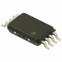
S-35390A-T8T1G Seiko Instruments, S-35390A-T8T1G Datasheet - Page 2

S-35390A-T8T1G
Manufacturer Part Number
S-35390A-T8T1G
Description
IC RTC I2C 2-WIRE 8-TSSOP
Manufacturer
Seiko Instruments
Type
Clock/Calendarr
Datasheet
1.S-35390A-J8T1G.pdf
(56 pages)
Specifications of S-35390A-T8T1G
Time Format
HH:MM:SS (12/24 hr)
Date Format
YY-MM-DD-dd
Interface
I²C, 2-Wire Serial
Voltage - Supply
1.3 V ~ 5.5 V
Operating Temperature
-40°C ~ 85°C
Mounting Type
Surface Mount
Package / Case
8-TSSOP
Function
Clock/Calendar/Alarm/Battery Backup/Interrupt
Supply Voltage (max)
5.5 V
Supply Voltage (min)
1.3 V
Maximum Operating Temperature
+ 85 C
Minimum Operating Temperature
- 40 C
Mounting Style
SMD/SMT
Rtc Bus Interface
Serial (2-Wire, I2C)
Lead Free Status / RoHS Status
Lead free / RoHS Compliant
Memory Size
-
Lead Free Status / Rohs Status
Lead free / RoHS Compliant
Other names
728-1007-2
Available stocks
Company
Part Number
Manufacturer
Quantity
Price
Company:
Part Number:
S-35390A-T8T1G
Manufacturer:
SEIKO
Quantity:
18 700
Part Number:
S-35390A-T8T1G
Manufacturer:
SEIKO
Quantity:
20 000
2
2-WIRE REAL-TIME CLOCK
S-35390A
Remark 1. x: G or U
Pin Configuration
List of Pin
Pin No.
1
2
3
4
5
6
7
8
2. Please select products of environmental code = U for Sn 100%, halogen-free products.
Symbol
XOUT
INT
INT
VDD
VSS
SDA
SCL
XIN
2
1
Output pin for
interrupt signal 1
Connection pin for
crystal oscillator
GND pin
Output pin for
interrupt signal 2
Input pin for serial
clock
I/O pin for serial data
Pin for positive power
supply
Description
Figure 2 Pin Configuration (S-35390A-T8T1x)
Figure 1 Pin Configuration (S-35390A-J8T1x)
Figure 3 Pin Configuration (S-35390A-I8T1x)
XOUT
INT1
VSS
XOUT
XIN
XOUT
INT1
INT1
VSS
VSS
XIN
XIN
Seiko Instruments Inc.
Bi-directional
8-Pin SOP (JEDEC)
1
2
3
4
Output
Output
1
2
3
4
Input
8-Pin TSSOP
I/O
−
−
−
1
2
3
4
Top view
Top view
Top view
SNT-8A
Table 1
Nch open-drain output
(no protective diode at VDD)
Nch open-drain output
(no protective diode at VDD)
CMOS input
(no protective diode at VDD)
Nch open-drain output
(no protective diode at VDD)
CMOS input
8
7
6
5
8
7
6
5
8
7
6
5
VDD
SDA
SCL
INT2
VDD
SDA
SCL
INT2
VDD
SDA
SCL
INT2
Configuration
−
−
−
Rev.3.0
_00


