DS1375T+T&R Maxim Integrated Products, DS1375T+T&R Datasheet - Page 2
DS1375T+T&R
Manufacturer Part Number
DS1375T+T&R
Description
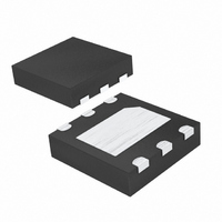
IC RTC SERIAL W/ALARM 6TDFN
Manufacturer
Maxim Integrated Products
Type
Clock/Calendar/Alarmr
Datasheet
1.DS1375T.pdf
(13 pages)
Specifications of DS1375T+T&R
Time Format
HH:MM:SS (12/24 hr)
Date Format
YY-MM-DD-dd
Interface
I²C, 2-Wire Serial
Voltage - Supply
1.7 V ~ 5.5 V
Operating Temperature
-40°C ~ 85°C
Mounting Type
Surface Mount
Package / Case
6-TDFN Exposed Pad
Lead Free Status / RoHS Status
Lead free / RoHS Compliant
Memory Size
-


ABSOLUTE MAXIMUM RATINGS
Voltage Range on V
Voltage Range on SDA, SCL, and WDS
Operating Temperature Range ...........................-40°C to +85°C
I
Stresses beyond those listed under “Absolute Maximum Ratings” may cause permanent damage to the device. These are stress ratings only, and functional
operation of the device at these or any other conditions beyond those indicated in the operational sections of the specifications is not implied. Exposure to
absolute maximum rating conditions for extended periods may affect device reliability.
RECOMMENDED DC OPERATING CONDITIONS
(V
wise noted.) (Note 1)
2
Note 1:
Note 2:
Note 3:
Note 4:
Note 5:
Note 6:
Note 7:
Supply Voltage
Timekeeping Voltage
Input Logic 1 (SDA, SCL)
Supply Voltage, Pullup
(SQW/INT, CLK)
Input Logic 0
Input Leakage (SCL, CLK)
I/O Leakage (SDA, SQW/INT)
SDA Logic 0 Output
SQW/INT Logic 0 Output
Active Supply Current
Standby Current
2
CC
Relative to Ground.............................................-0.3V to +6.0V
Relative to Ground ....................................-0.3V to V
C Digital Input RTC with Alarm
_____________________________________________________________________
= +1.7V to +5.5V, T
PARAMETER
Limits at -40°C are guaranteed by design and not production tested.
All voltages are referenced to ground.
For the CLK pin, input voltages above V
exceed the current drawn by the circuit that is connected to V
voltage level on the V
V
I
CLK pin running at 32,768Hz, rise and fall times at 10ns or less.
Specified with I
CCA
IL MIN
—SCL clocking at max frequency = 400kHz.
on the CLK pin can exceed -0.3V as long as the current is limited to less than 1mA.
CC
Pin
A
2
= -40°C to +85°C, unless otherwise noted. Typical values are at V
C bus inactive.
CC
bus.
SYMBOL
V
I
I
OLSQW
PULLUP
OLSDA
I
I
V
V
V
CCA
CCS
V
I
I
LO
CC
TK
LI
IH
IL
(Note 2)
(Note 2)
(Note 2)
(Notes 2, 3)
(Notes 2, 4)
V
V
V
1.7V < V
1.3V < V
(Notes 5, 6)
(Notes 6, 7)
CC
CC
CC
CC
CC
> 2V; V
< 2V; V
> 2V; V
+ 0.3V cause current to flow into the device. The input current must not
+ 0.3V
CC
CC
< 2V; V
< 1.7V; V
OL
OL
OL
CONDITIONS
= 0.4V
= 0.2 x V
= 0.4V
OL
Storage Temperature Range .............................-55°C to +125°C
Soldering Temperature...........................Refer to the IPC/JEDEC
OL
= 0.2 x V
CC
CC
= 0.2 x V
. Otherwise, current flows out of the DS1375, raising the
CC
CC
CC
0.7 x V
MIN
-0.3
1.7
1.3
-1
-1
= 3.3V, T
CC
TYP
150
3.3
33
A
J-STD-020 Specification.
= +25°C, unless other-
V
CC
MAX
+0.3
V
250
150
500
+ 0.3
5.5
5.5
5.5
3.0
3.0
+1
+1
CC
UNITS
mA
mA
µA
µA
µA
µA
nA
V
V
V
V
V
Related parts for DS1375T+T&R
Image
Part Number
Description
Manufacturer
Datasheet
Request
R

Part Number:
Description:
IC RTC SERIAL W/ALARM 6-TDFN
Manufacturer:
Maxim Integrated Products
Datasheet:

Part Number:
Description:
Real Time Clock
Manufacturer:
Maxim Integrated Products
Datasheet:
Part Number:
Description:
Real Time Clock
Manufacturer:
Maxim Integrated Products
Datasheet:

Part Number:
Description:
Ds13 D-sub Dual Port Type
Manufacturer:
Megastar Electronics Inc.
Datasheet:
Part Number:
Description:
DS13 Series High Performance Solid State Relays For Loads Up To 2A@60Vdc
Manufacturer:
MACOM [Tyco Electronics]
Datasheet:

Part Number:
Description:
Solid State Relays HIGH FREQUENCY RELAY
Manufacturer:
Tyco Electronics

Part Number:
Description:
DS13-1002 = DS13 SOLID STATE D
Manufacturer:
TE Connectivity
Datasheet:
Part Number:
Description:
MAX7528KCWPMaxim Integrated Products [CMOS Dual 8-Bit Buffered Multiplying DACs]
Manufacturer:
Maxim Integrated Products
Datasheet:
Part Number:
Description:
Single +5V, fully integrated, 1.25Gbps laser diode driver.
Manufacturer:
Maxim Integrated Products
Datasheet:
Part Number:
Description:
Single +5V, fully integrated, 155Mbps laser diode driver.
Manufacturer:
Maxim Integrated Products
Datasheet:
Part Number:
Description:
VRD11/VRD10, K8 Rev F 2/3/4-Phase PWM Controllers with Integrated Dual MOSFET Drivers
Manufacturer:
Maxim Integrated Products
Datasheet:
Part Number:
Description:
Highly Integrated Level 2 SMBus Battery Chargers
Manufacturer:
Maxim Integrated Products
Datasheet:
Part Number:
Description:
Current Monitor and Accumulator with Integrated Sense Resistor; ; Temperature Range: -40°C to +85°C
Manufacturer:
Maxim Integrated Products