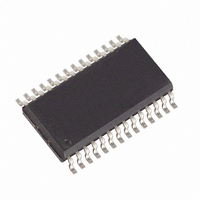
DS1501YZ+ Maxim Integrated Products, DS1501YZ+ Datasheet - Page 11

DS1501YZ+
Manufacturer Part Number
DS1501YZ+
Description
IC RTC WDOG Y2KC 5.0V 28-SOIC
Manufacturer
Maxim Integrated Products
Type
Clock/Calendar/WDT/NVSRAM/Y2Kr
Datasheet
1.DS1501WE.pdf
(22 pages)
Specifications of DS1501YZ+
Memory Size
2K (256 x 8)
Time Format
HH:MM:SS (24 hr)
Date Format
YY-MM-DD-dd
Interface
Parallel
Voltage - Supply
4.5 V ~ 5.5 V
Operating Temperature
0°C ~ 70°C
Mounting Type
Surface Mount
Package / Case
28-SOIC (7.5mm Width)
Lead Free Status / RoHS Status
Lead free / RoHS Compliant
DETAILED DESCRIPTION
The DS1501/DS1511 RTC is a low-power clock/date device with a programmable day of week/date alarm. The
DS1501/DS1511 is accessed through a parallel interface. The clock/date provides seconds, minutes, hours, day,
date, month, and year information. The date at the end of the month is automatically adjusted for months with
fewer than 31 days, including corrections for leap year.
The RTC registers are double buffered into an internal and external set. The user has direct access to the external
set. Clock/calendar updates to the external set of registers can be disabled and enabled to allow the user to access
static data. When the crystal oscillator is turned on, the internal set of registers are continuously updated; this
occurs regardless of external register settings to guarantee that accurate RTC information is always maintained.
The DS1501/DS1511 contain their own power-fail circuitry that automatically deselects the device when the V
supply falls below a power-fail trip point. This feature provides a high degree of data security during unpredictable
system operation caused by low V
The DS1501/DS1511 have interrupt (IRQ), power control (PWR), and reset (RST) outputs that can be used to
control CPU activity. The IRQ interrupt or RST outputs can be invoked as the result of a time-of-day alarm, CPU
watchdog alarm, or a kickstart signal. The DS1501/DS1511 power-control circuitry allow the system to be powered
on by an external stimulus, such as a keyboard or by a time and date (wakeup) alarm. The PWR output pin can be
triggered by one or either of these events, and can be used to turn on an external power supply. The PWR pin is
under software control, so that when a task is complete, the system power can then be shut down. The
DS1501/DS1511 power-on reset can be used to detect a system power-down or failure and hold the CPU in a safe
reset state until normal power returns and stabilizes; the RST output is used for this function.
The DS1501/DS1511 are clock/calendar chips with the features described above. An external crystal and battery
are the only components required to maintain time-of-day and memory status in the absence of power.
Table 1. RTC Operating Modes
DATA READ MODE
The DS1501/DS1511 are in read mode whenever CE (chip enable) and OE (output enable) are low and WE (write
enable) is high. The device architecture allows ripple-through access to any valid address location. Valid data is
available at the DQ pins within t
access times are satisfied. If CE or OE access times are not met, valid data is available at the latter of chip-enable
access (t
and OE. If the outputs are activated before t
address inputs are changed while CE and OE remain valid, output data remains valid for output-data hold time (t
but then goes indeterminate until the next address access (Table 1).
DATA WRITE MODE
The DS1501/DS1511 are in write mode whenever CE and WE are in their active state. The start of a write is
referenced to the latter occurring transition of CE or WE. The addresses must be held valid throughout the cycle.
CE or WE must return inactive for a minimum of t
in must be valid t
signal is high during a write cycle. However, OE can be active provided that care is taken with the data bus to avoid
bus contention. If OE is low prior to a high-to-low transition on WE, the data bus can become active with read data
defined by the address inputs. A low transition on WE then disables the outputs t
V
V
SO
CC
In tolerance
< V
< V
V
CSA
CC
CC
SO
) or at output-enable access time (t
< V
< V
PF
PF
DS
prior to the end of the write and remain valid for t
CE
V
V
V
V
X
X
IH
IL
IL
IL
AA
OE
V
V
X
X
X
X
IH
CC
IL
(address access) after the last address input is stable, provided that CE and OE
levels.
WE
V
V
V
X
X
X
IH
IH
IL
AA
OEA
, the data lines are driven to an intermediate state until t
DQ0–DQ7
WR
). The state of the data input/output pins (DQ) is controlled by CE
High-Z
High-Z
High-Z
High-Z
D
prior to the initiation of a subsequent read or write cycle. Data
D
OUT
IN
11 of 22
DS1501/DS1511 Y2KC Watchdog Real-Time Clocks
A0–A4
A
A
A
X
X
X
IN
IN
IN
DH
afterward. In a typical application, the OE
Data Retention
Deselect
Deselect
MODE
Write
Read
Read
WEZ
after WE goes active (Table 1).
CMOS Standby
Battery Current
POWER
Standby
Active
Active
Active
AA
. If the
OH
CC
)


