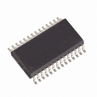
DS1501YZ+ Maxim Integrated Products, DS1501YZ+ Datasheet - Page 18

DS1501YZ+
Manufacturer Part Number
DS1501YZ+
Description
IC RTC WDOG Y2KC 5.0V 28-SOIC
Manufacturer
Maxim Integrated Products
Type
Clock/Calendar/WDT/NVSRAM/Y2Kr
Datasheet
1.DS1501WE.pdf
(22 pages)
Specifications of DS1501YZ+
Memory Size
2K (256 x 8)
Time Format
HH:MM:SS (24 hr)
Date Format
YY-MM-DD-dd
Interface
Parallel
Voltage - Supply
4.5 V ~ 5.5 V
Operating Temperature
0°C ~ 70°C
Mounting Type
Surface Mount
Package / Case
28-SOIC (7.5mm Width)
Lead Free Status / RoHS Status
Lead free / RoHS Compliant
DS1501/DS1511 Y2KC Watchdog Real-Time Clocks
The interrupt flag bit (either TDF or KSF) associated with the attempted power-on sequence remains set until
cleared by software during a subsequent system power-on.
If V
is applied within the timeout period, the system power-on sequence continues, as shown in Intervals 2 to 5 in
CC
the timing diagram. During Interval 2, PWR remains active, and IRQ is driven to its active-low level, indicating that
either TDF or KSF was set in initiating the power-on. In the diagram, KS is assumed to be pulled up to the V
BAUX
supply. Also at this time, the PAB bit is automatically cleared to 0 in response to a successful power-on. The PWR
line remains active as long as the PAB remains cleared to 0.
At the beginning of Interval 3, the system processor has begun code execution and clears the interrupt condition of
TDF and/or KSF by reading the flags register or by writing TDF and KSF to 0. As long as no other interrupt within
the DS1501/DS1511 is pending, the IRQ line is taken inactive once these bits are reset, and execution of the
application software can proceed. During this time, the wakeup and kickstart functions can be used to generate
status and interrupts. TDF is set in response to a day/date, hours, minutes, and seconds match condition. KSF is
set in response to a low-going transition on KS. If the associated interrupt-enable bit is set (TDE and/or KIE), then
the IRQ line is driven low in response to enabled event. In addition, the other possible interrupt sources within the
DS1501/DS1511 can cause IRQ to be driven low. While system power is applied, the on-chip logic always attempts
to drive the PWR pin active in response to the enabled kickstart or wakeup condition. This is true even if PWR was
previously inactive as the result of power being applied by some means other than wakeup or kickstart.
The system can be powered down under software control by setting the PAB bit to 1. The PAB bit can only be set
to 1 after the TDF and KSF flags have been cleared to 0. Setting PAB to 1 causes the open-drain PWR pin to be
placed in a high-impedance state, as shown at the beginning of Interval 4 in the timing diagram. As V
voltage
CC
decays, the IRQ output pin is placed in a high-impedance state when V
goes below V
. If the system is to be
CC
PF
again powered on in response to a wakeup or kickstart, then both the TDF and KSF flags should be cleared, and
TPE and/or KIE should be enabled prior to setting the PAB bit.
During Interval 5, the system is fully powered down. Battery backup of the clock calendar and NV RAM is in effect
and IRQ is tri-stated, and monitoring of wakeup and kickstart takes place. If PRS = 1, PWR stays active; otherwise,
if PRS = 0, PWR is tri-stated.
SQUARE-WAVE OUTPUT
The square-wave output is enabled and disabled through the E32K bit. If the square wave is enabled (E32K = 0)
and the oscillator is running, then a 32.768kHz square wave is output on the SQW pin. If the battery-backup
32kHz-enable bit (BB32) is enabled, and voltage is applied to V
, then the 32.768kHz square wave is output on
BAUX
the SQW pin in the absence of V
.
CC
BATTERY MONITOR
The DS1501/DS1511 constantly monitor the battery voltage of the backup-battery sources (V
and V
). The
BAT
BAUX
battery low flags BLF1 and BLF2 are set to 1 if the battery voltages on V
and V
are less than V
(typical);
BAT
BAUX
BLF
otherwise, BLF1 and BLF2 are 0. BLF1 monitors V
and BLF2 monitors V
.
BAT
BAUX
256 x 8 EXTENDED RAM
Two on-chip latch registers control access to the SRAM. One register is used to hold the SRAM address; the other
is used to hold read/write data. The SRAM address space is from 00h to FFh. The 8-bit address of the RAM
location to be accessed must be loaded into the extended RAM address register located at 10h. Data in the
addressed location can be read by performing a read operation from location 13h, or written to by performing a
write operation to location 13h. Data in any addressed location can be read or written repeatedly with changing the
address in location 10h.
To read or write consecutive extended RAM locations, a burst mode feature can be enabled to increment the
extended RAM address. To enable the burst mode feature, set the BME bit to 1. With burst mode enabled, write
the extended RAM starting address location to register 10h. Then read or write the extended RAM data from/to
register 13h. The extended RAM address locations are automatically incremented on the rising edge of OE, CE, or
18 of 22


