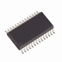
DS1501YZ+ Maxim Integrated Products, DS1501YZ+ Datasheet - Page 17

DS1501YZ+
Manufacturer Part Number
DS1501YZ+
Description
IC RTC WDOG Y2KC 5.0V 28-SOIC
Manufacturer
Maxim Integrated Products
Type
Clock/Calendar/WDT/NVSRAM/Y2Kr
Datasheet
1.DS1501WE.pdf
(22 pages)
Specifications of DS1501YZ+
Memory Size
2K (256 x 8)
Time Format
HH:MM:SS (24 hr)
Date Format
YY-MM-DD-dd
Interface
Parallel
Voltage - Supply
4.5 V ~ 5.5 V
Operating Temperature
0°C ~ 70°C
Mounting Type
Surface Mount
Package / Case
28-SOIC (7.5mm Width)
Lead Free Status / RoHS Status
Lead free / RoHS Compliant
DS1501/DS1511 Y2KC Watchdog Real-Time Clocks
is powered by either V
, V
, or V
. If either watchdog register is nonzero, a timeout sets the WDF bit to 1,
CC
BAT
BAUX
regardless of the state of the watchdog enable (WDE) bit, to serve as an indication to the processor that a
watchdog timeout has occurred. The watchdog timer operates in two modes, repetitive and single-shot.
If WDE is 1 and the watchdog steering bit (WDS) is 0, the watchdog is in repetitive mode. When the watchdog
times out, both WDF and IRQF are set. IRQ goes active and IRQF goes to 1. The watchdog timer is reloaded when
the processor performs a write of the watchdog registers and the timeout period restarts. Reading control A register
clears the IRQ flag.
If WDE and WDS are 1, the watchdog is in single-shot mode. When the watchdog times out, RST goes active for a
period of 40ms to 200ms. When RST goes inactive, WDE resets to 0. Writing a value of 00h to both watchdog
registers disables the watchdog timer. The watchdog function is automatically disabled upon power-up by the
power-on reset setting WDE = 0 and WDS = 0. The watchdog registers are not initialized at power-up and should
be initialized by the user.
Note: The TE bit must be used to disable transfers when writing to the watchdog registers.
The following summarizes the configurations in which the watchdog can be used:
WDE = 0 and WDS = 0: WDF is set.
WDE = 0 and WDS = 1: WDF is set.
WDE = 1 and WDS = 0: WDF and IRQF are set, and the IRQ pin is pulled low.
WDE = 1 and WDS = 1: WDF is set, the RST pin pulses low, and WDE resets to 0.
WAKEUP/KICKSTART
The DS1501/DS1511 incorporate a wakeup feature, which powers on at a predetermined day/date and time by
activating the PWR output pin. Additionally, the kickstart feature allows the system to be powered up in response to
a low-going transition on the KS pin, without operating voltage applied to the V
pin. As a result, system power
CC
can be applied upon such events as key closure or a modem-ring-detect signal. To use either the wakeup or the
kickstart features, the DS1501DS1511 must have an auxiliary battery connected to the V
pin, and the oscillator
BAUX
must be running.
The wakeup feature is controlled through the time-of-day/date power-enable bit (TPE). Setting TPE to 1 enables
the wakeup feature. Transfers (TE) must be enabled for a wake up event to occur. Writing TPE to 0 disables the
wakeup feature. The kickstart feature is always enabled as long as V
is present.
BAUX
If the wakeup feature is enabled, while the system is powered down (no V
voltage), the clock/calendar monitors
CC
the current day or date for a match condition with day/date alarm register (0Bh). With the day/date alarm register,
the hours, minutes, and seconds alarm bytes in the clock/calendar register map (02h, 01h, and 00h) are also
monitored. As a result, a wakeup occurs at the day or date and time specified by the day/date, hours, minutes, and
seconds alarm register values. This additional alarm occurs regardless of the programming of the TIE bit. When the
match condition occurs, the PWR pin is automatically driven low. This output can turn on the main system power
supply that provides V
voltage to the DS1501/DS1511, as well as the other major components in the system.
CC
Also at this time, the time-of-day/date alarm flag is set (TDF), indicating a wakeup condition has occurred.
is low, the KS input pin is monitored for a low-going transition of minimum pulse width
If V
is present, while V
BAUX
CC
. When such a transition is detected, the PWR line is pulled low, as it is for a wakeup condition. Also at this
t
KSPW
time, KSF is set, indicating that a kickstart condition has occurred. The KS input pin is always enabled and must not
be allowed to float.
The timing associated with the wakeup and kickstarting sequences is illustrated in Figure 7. These functions are
divided into five intervals, labeled 1 to 5 on the diagram.
The occurrence of either a kickstart or wakeup condition causes the PWR pin to be driven low, as described above.
During Interval 1, if the supply voltage on the V
pin rises above V
before the power-on timeout period (t
)
CC
SO
POTO
expires, then PWR remains at the active-low level. If V
in this time, then the PWR
does not rise above the V
CC
SO
output pin is turned off and returns to its high-impedance level. In this event, the IRQ pin also remains tri-stated.
17 of 22


