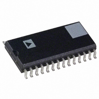
AD73322LAR-REEL Analog Devices Inc, AD73322LAR-REEL Datasheet - Page 16

AD73322LAR-REEL
Manufacturer Part Number
AD73322LAR-REEL
Description
IC ANALOG FRONT END DUAL 28-SOIC
Manufacturer
Analog Devices Inc
Specifications of AD73322LAR-REEL
Rohs Status
RoHS non-compliant
Number Of Bits
16
Number Of Channels
4
Power (watts)
73mW
Voltage - Supply, Analog
2.7 V ~ 5.5 V
Voltage - Supply, Digital
2.7 V ~ 5.5 V
Package / Case
28-SOIC (7.5mm Width)
Single Supply Voltage (min)
2.7V
Single Supply Voltage (max)
3.3V
Package Type
SOIC W
Lead Free Status / RoHS Status
Not Compliant
AD73322L
Serial Clock Rate Divider
The AD73322L features a programmable serial clock divider
that allows users to match the serial clock (SCLK) rate of the
data to that of the DSP engine or host processor. The maximum
SCLK rate available is DMCLK and the other available rates
are: DMCLK/2, DMCLK/4 and DMCLK/8. The slowest rate
(DMCLK/8) is the default SCLK rate. The serial clock divider
is programmable by setting bits CRB:2–3. Table VIII shows the
serial clock rate corresponding to the various bit settings.
Sample Rate Divider
The AD73322L features a programmable sample rate divider
that allows users flexibility in matching the codec’s ADC and
DAC sample rates (decimation/interpolation rates) to the needs
of the DSP software. The maximum sample rate available is
DMCLK/256, which offers the lowest conversion group delay,
while the other available rates are: DMCLK/512, DMCLK/
1024 and DMCLK/2048. The slowest rate (DMCLK/2048) is
the default sample rate. The sample rate divider is program-
mable by setting bits CRB:0-1. Table IX shows the sample
rate corresponding to the various bit settings.
Table VIII. SCLK Rate Divider Settings
SCD1
0
0
1
1
SCD0
0
1
0
1
SCLK Rate
DMCLK/8
DMCLK/4
DMCLK/2
DMCLK
DAC Advance Register
The loading of the DAC is internally synchronized with the
unloading of the ADC data in each sampling interval. The
default DAC load event happens one SCLK cycle before the
SDOFS flag is raised by the ADC data being ready. However,
this DAC load position can be advanced before this time by
modifying the contents of the DAC advance field in Control
Register E (CRE:0–4). The field is five bits wide, allowing 31
increments of weight 1/(F
F
the Sample Rate divider; see Tables VII and IX. In certain cir-
cumstances this DAC update adjustment can reduce the group
delay when the ADC and DAC are used to process data in series.
Appendix C details how the DAC advance feature can be used.
NOTE: The DAC advance register should not be changed while
the DAC section is powered up.
DA4
0
0
0
1
1
S
is dependent on the setting of both the MCLK divider and
DA3
0
0
0
1
1
Table IX. Sample Rate Divider Settings
DIR1
0
0
1
1
Table X. DAC Timing Control
DA2
0
0
0
1
1
DIR0
0
1
0
1
S
× 32); see Table X. The sample rate
DA1
0
0
1
1
1
SCLK Rate
DMCLK/2048
DMCLK/1024
DMCLK/512
DMCLK/256
DA0
0
1
0
0
1
Time Advance
0 s
1/(F
2/(F
30/(F
31/(F
S
S
S
S
× 32) s
× 32) s
× 32) s
× 32) s


